Bill and Will's Synth
|
||||||||||||||||||||||||||||||||||||||||||||||||||||||||||||||||||||||||||||||||||||||||||||||||||||||||||||||||||||||||||||||||||||||||||||||||||||||||||||||||||||||||||||||||||||||||||||||||||||||||||||||||||||||||
Table of Contents |
||||||||||||||||||||||||||||||||||||||||||||||||||||||||||||||||||||||||||||||||||||||||||||||||||||||||||||||||||||||||||||||||||||||||||||||||||||||||||||||||||||||||||||||||||||||||||||||||||||||||||||||||||||||||
|
This page has become really long, so here's a table of contents that we hope will make it easier to traverse: Background - presents an explanation and Ken Stone's initial description of the Module with his photos Modifications - presents details of the different possible implementations Parts - presents a Bill of Materials and notes about it Panel - presents the MOTM format panel Construction Phase 1 - Resistors, Capacitors, IC Sockets, Power Plugs, MTA headers Construction Phase 2 - Trimmers, Tube, Panel connetcions |
||||||||||||||||||||||||||||||||||||||||||||||||||||||||||||||||||||||||||||||||||||||||||||||||||||||||||||||||||||||||||||||||||||||||||||||||||||||||||||||||||||||||||||||||||||||||||||||||||||||||||||||||||||||||
|
Background - Yves' Original 12 Band Design |
||||||||||||||||||||||||||||||||||||||||||||||||||||||||||||||||||||||||||||||||||||||||||||||||||||||||||||||||||||||||||||||||||||||||||||||||||||||||||||||||||||||||||||||||||||||||||||||||||||||||||||||||||||||||
|
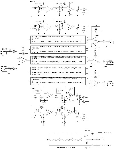
Here's Yves' Schematic (click here to download a larger version):
Here's the layout of his PCB (this is Yves' illustration - thanks, Yves):
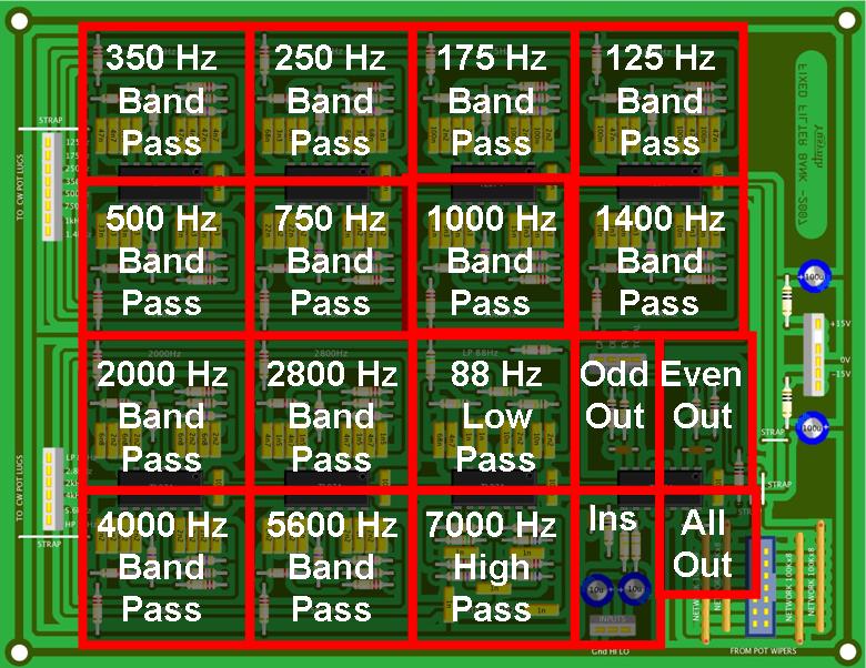
Here's how the filters lay out on his PCB:
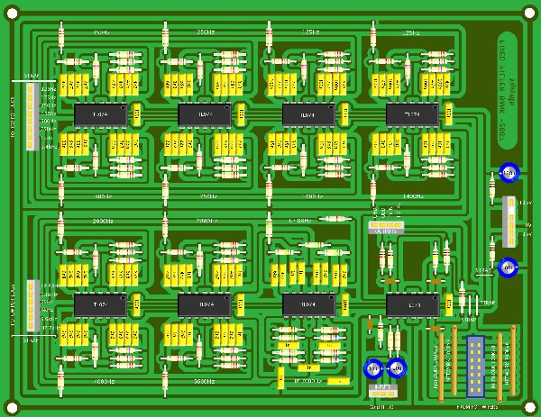
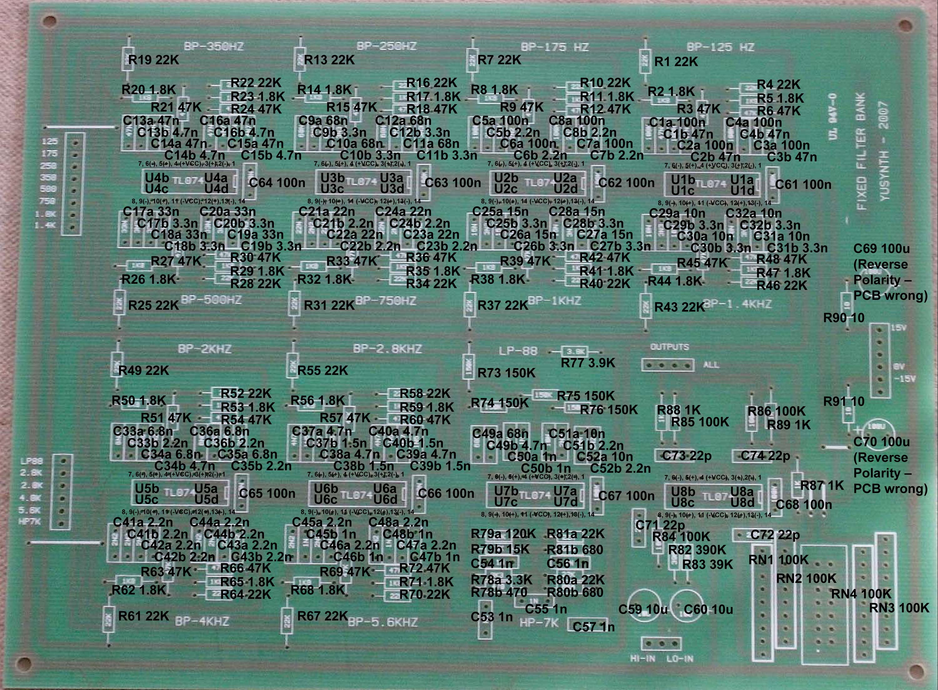
This is an annotated image we made of the PCB showing the Resistors, Capacitors, ICs etc. by name and value. Click on the image to see a larger (and legible) version (133K):
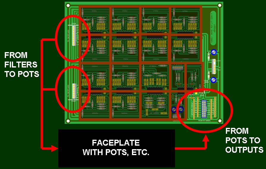
Click here for a high-resolution jpeg version (890K) Click here for a high-resolution pdf version (250K) The filtered signal goes to and from the face-plate potentiometers like this:
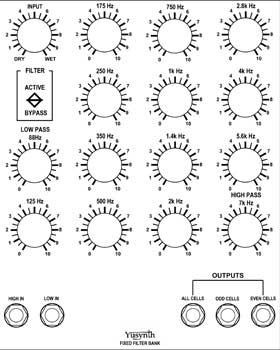
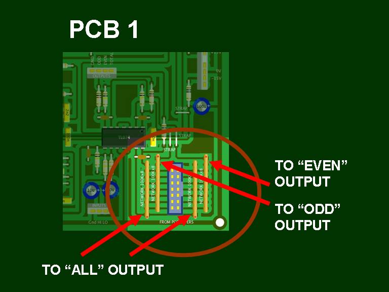
From the face-plate potentiometers, the signal gets divided into three discrete outputs - "Odd," "Even," and "All":
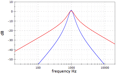
Yves has built each filter with two Op Amps to get a narrow bandwitdh and steep slope. Here is Yves' diagram of the predicted slope of the band pass filter at the 1K Hz point:
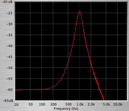
Yves writes: "The red curve corresponds to the spectrum at the output of the first OPA. As it can be seen, the lowpass and highpass slopes are -6dB/octave (-20dB/decade), Q=2.7. "The blue curve corresponds to the spectrum at the output of the second OPA. Here we obtain a narrower bandwith Q=4, as well as steeper slopes, -12dB/octave (-40dB/decade)" Here is Yves' spectrum measurement at 1K Hz band pass he made on his module prototype using a "white" noise source and measured with the SignalScope software (valuation version, on Macintosh MacOSX)
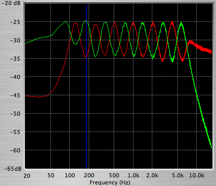
And is Yves' spectrum measurement of the Odd (Red) and Even (Green) outputs
|
||||||||||||||||||||||||||||||||||||||||||||||||||||||||||||||||||||||||||||||||||||||||||||||||||||||||||||||||||||||||||||||||||||||||||||||||||||||||||||||||||||||||||||||||||||||||||||||||||||||||||||||||||||||||
Modifications |
||||||||||||||||||||||||||||||||||||||||||||||||||||||||||||||||||||||||||||||||||||||||||||||||||||||||||||||||||||||||||||||||||||||||||||||||||||||||||||||||||||||||||||||||||||||||||||||||||||||||||||||||||||||||
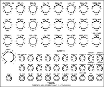
1. 22 Band Modification |
||||||||||||||||||||||||||||||||||||||||||||||||||||||||||||||||||||||||||||||||||||||||||||||||||||||||||||||||||||||||||||||||||||||||||||||||||||||||||||||||||||||||||||||||||||||||||||||||||||||||||||||||||||||||
|
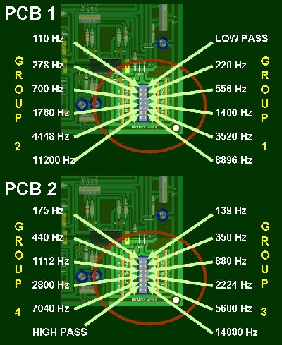
We were interested in building a filter with more band-pass filters. We want to experiment with what this kind of filter can do given a wider range. Yves' design uses band-pass center frequencies that are approximately 1/2 octave apart - 125hz, 175hz, 250hz, etc. And it looked to us like if we divided his center points in half - well - 4 frequencies per octave would seem crowded unless the slopes were increased. That would require another Op Amp per filter - couldn't do it in the context of his circuit designs and PCBs. And also, whereas it might increase the "granularity" of the filter, it wouldn't really expand the range of the filter. But it looked to us like if we increased the number of bands so there'd be 3 bands per octave instead of 2 - or if each band was 1/3 of an octave apart... that would be pretty good. So we calculated frequencies using (A4) 440 Hz as a starting point because it was easy given our resources. Yves took a look at it and suggested the following set-up:
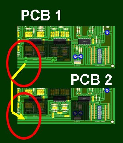
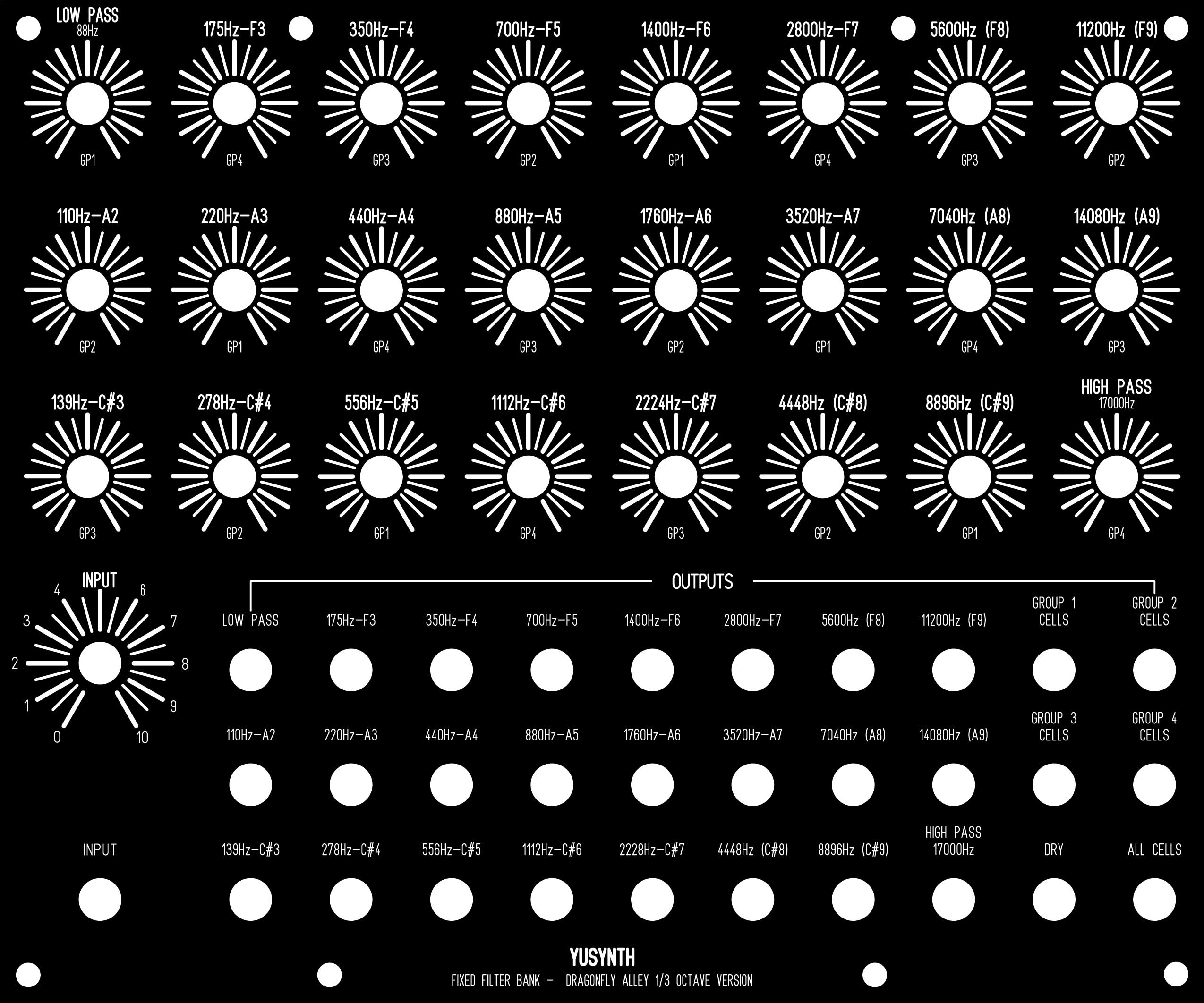
So - to achieve the 22 band 1/3 octave version with the Outputs by "Group" (rather than even/odd) here's how we arranged the filters, etc on the two PCBs required. The reason we divided the filters this way between the boards has to do with how we're planning to attach the boards behind the panels - PCB 2 on the left side (looking at the back, that's the high-pass filter side) - PCB 1 on the right side (looking at the back, that's the low-pass filter side):
We'll have to run a jumper from the input buss on PCB1 to the input buss on PCB 2 like this:
| ||||||||||||||||||||||||||||||||||||||||||||||||||||||||||||||||||||||||||||||||||||||||||||||||||||||||||||||||||||||||||||||||||||||||||||||||||||||||||||||||||||||||||||||||||||||||||||||||||||||||||||||||||||||||
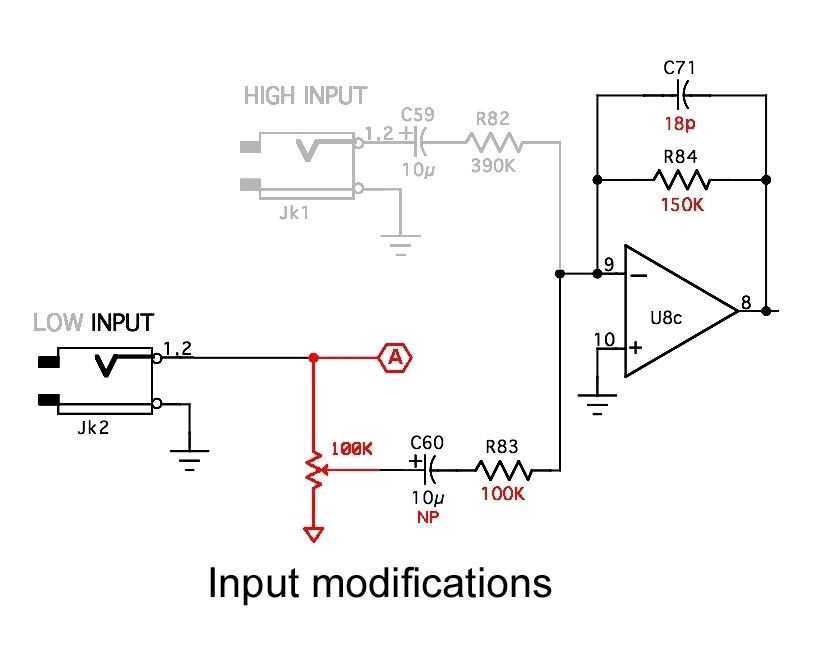
2. Input Attenuation Modification |
||||||||||||||||||||||||||||||||||||||||||||||||||||||||||||||||||||||||||||||||||||||||||||||||||||||||||||||||||||||||||||||||||||||||||||||||||||||||||||||||||||||||||||||||||||||||||||||||||||||||||||||||||||||||
|
Yves' design has two inputs - a high and a low. Dave Brown came up with an attenuated input option. We decided to implement the design that way:
| ||||||||||||||||||||||||||||||||||||||||||||||||||||||||||||||||||||||||||||||||||||||||||||||||||||||||||||||||||||||||||||||||||||||||||||||||||||||||||||||||||||||||||||||||||||||||||||||||||||||||||||||||||||||||
|
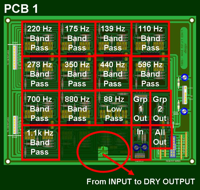
3. Dry Output Modification |
||||||||||||||||||||||||||||||||||||||||||||||||||||||||||||||||||||||||||||||||||||||||||||||||||||||||||||||||||||||||||||||||||||||||||||||||||||||||||||||||||||||||||||||||||||||||||||||||||||||||||||||||||||||||
|
We decided to include a separate, dry output from the input buss. We'll send the output through a buffer/inverter on the way to its jack on the panel.
|
||||||||||||||||||||||||||||||||||||||||||||||||||||||||||||||||||||||||||||||||||||||||||||||||||||||||||||||||||||||||||||||||||||||||||||||||||||||||||||||||||||||||||||||||||||||||||||||||||||||||||||||||||||||||
|
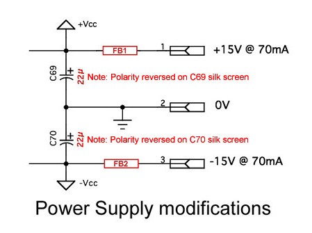
4. Power Supply Modification |
||||||||||||||||||||||||||||||||||||||||||||||||||||||||||||||||||||||||||||||||||||||||||||||||||||||||||||||||||||||||||||||||||||||||||||||||||||||||||||||||||||||||||||||||||||||||||||||||||||||||||||||||||||||||
|
We decided to include a modification to the power supply - Will had already figured out what we'd do (a-la the Tau Pipe), but Dave Brown's already got pictures and all. Here's his schematic:
Here are Dave's pictures of his implementation of this mod:
|
||||||||||||||||||||||||||||||||||||||||||||||||||||||||||||||||||||||||||||||||||||||||||||||||||||||||||||||||||||||||||||||||||||||||||||||||||||||||||||||||||||||||||||||||||||||||||||||||||||||||||||||||||||||||
|
5. Filter POT Modification |
||||||||||||||||||||||||||||||||||||||||||||||||||||||||||||||||||||||||||||||||||||||||||||||||||||||||||||||||||||||||||||||||||||||||||||||||||||||||||||||||||||||||||||||||||||||||||||||||||||||||||||||||||||||||
|
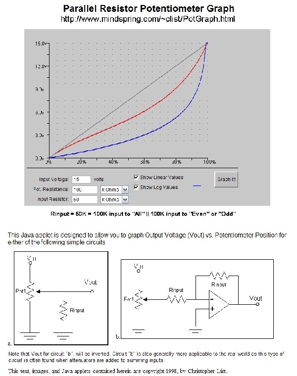
When we saw Dave Brown had used 100k linear pots - rather then the 10k log POTs Yves specified - we asked him about it. Here's what he said (very interesting): "Several thoughts on this. "First, log pots are more 'contoured' to how we hear volume. This gives the control a more linear volume 'feel'... "The input to the mixer is 100K. When using 10K log pots, the input impedance is 10X and so becomes negligible. However, when using 100K pots, the input impedance is equal to the pot and so becomes a factor. It affects the contour and actually makes it sound more like a log pot. There is some information on the in the section "Changing the Law of a Pot" on http://sound.westhost.com/pots.htm "In this case, "R" is the input impedance of the circuit, which is the 100K series resistor to the op amp. There is a neat graphing page at Christopher List's site: http://www.mindspring.com/~clist/PotGraph.html, which will show that with 100K for each resistor, the response is 1/3 of the way to a log potentiometer.
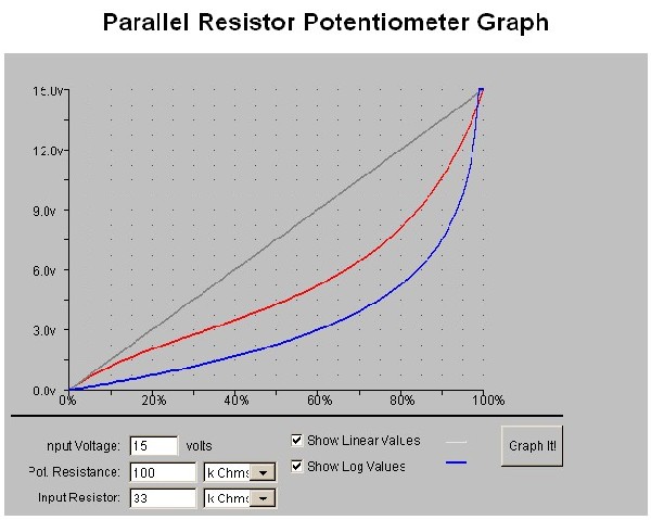
"For my mixers, I generally want linear because I can "add" the values to make sure I'm not overloading the output. The stock MOTM-830 mixer has the gain adjusted down so you won't exceed ±5 volts with 6 inputs. I've changed them all back to a gain of 1 which will greatly overload. But, I know with 3 inputs, the sum generally has to be 10, so one at 5 and two at 2.5 is generally close. It's not perfect, but generally it's close enough and very difficult with log potentiometers. Note that with this filter, this isn't the case since you are never adding like frequencies and the gain of each filter is one. "Note that the lowpass has a series resistor R77 and the highpass has a series capacitor C57. R77 decreases the gain of the lowpass, and 3K9 with a 100K potentiometer is negligible so my lowpass is boosted a bit. C57 provides a highpass filter, and increasing the resistance with a 100K potentiometer significantly shifts the cutoff. I haven't played enough with this filter to decide if I want to adjust those values. It's somewhat confusing because Yves has both 10K and 25K labels on those potentiometers. I figure I can fine tune it later if I want. On the bench, it sounded fine. "I tried it just as the PCB with 100K linear potentiometers and it felt / sounded just fine... "Dave" So as we were looking over that explanation of his use of the 100K linear POTs - specifically, the chart above showing the effect of the 50K resistance on the POT output. We think he's saying that each POT goes to two resistors in parallel - these are the resistor networks - each 100K. And these are the input resistances to the output amps. So - we get it - two 100k resistors in series would be 200k - totally makes sense. So two 100k resistors in parallel makes 50K. Also makes sense. Now, we're going to take the individual outputs pre-potentiometer... but if you decide to take the individual outputs post-potentiometer, each POT will go to three 100k resistances... the "Total Network" (RN1 or RN4), the "Group Network" (RN2 or RN3 on PCB1 and PCB2), and the 100K input resistor to an individual output buffer. These 100k resistors in parallel would make a resistance of 33.33k. So we plugged 33k value into the gadget at Christopher List's site: http://www.mindspring.com/~clist/PotGraph.html, and the resultant curve looks a little curvier - but not too radical. If anything it looks a might bit more logarithmic. So if you do it that way, you're cool with that <G>.
|
||||||||||||||||||||||||||||||||||||||||||||||||||||||||||||||||||||||||||||||||||||||||||||||||||||||||||||||||||||||||||||||||||||||||||||||||||||||||||||||||||||||||||||||||||||||||||||||||||||||||||||||||||||||||
|
6. Output Groups Modification |
||||||||||||||||||||||||||||||||||||||||||||||||||||||||||||||||||||||||||||||||||||||||||||||||||||||||||||||||||||||||||||||||||||||||||||||||||||||||||||||||||||||||||||||||||||||||||||||||||||||||||||||||||||||||
|
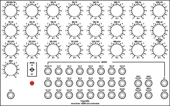
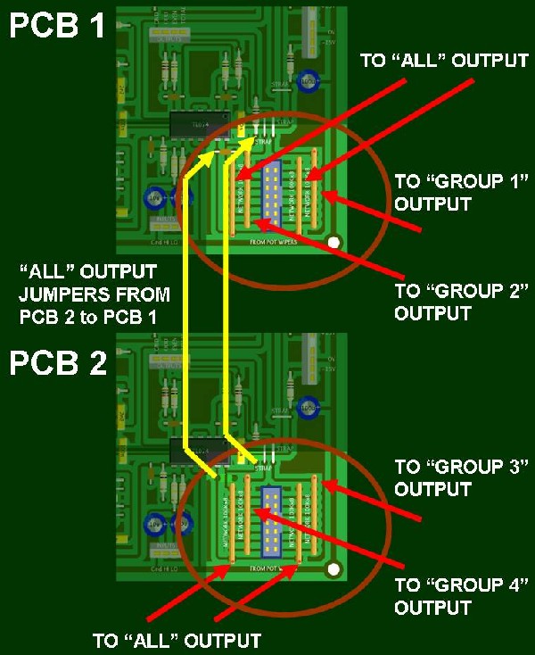
Yves' design has three output groups - "Even" "Odd" and "All." Since we have two FFB PCBs, we've got the potential for four groups. Why not use them? Here's how the groups stack up:
The outputs from the panel control pots come into the groups like this:
And here's how the outputs of these groups get implemented:
|
||||||||||||||||||||||||||||||||||||||||||||||||||||||||||||||||||||||||||||||||||||||||||||||||||||||||||||||||||||||||||||||||||||||||||||||||||||||||||||||||||||||||||||||||||||||||||||||||||||||||||||||||||||||||
|
7. Separate Band output Modification |
||||||||||||||||||||||||||||||||||||||||||||||||||||||||||||||||||||||||||||||||||||||||||||||||||||||||||||||||||||||||||||||||||||||||||||||||||||||||||||||||||||||||||||||||||||||||||||||||||||||||||||||||||||||||
|
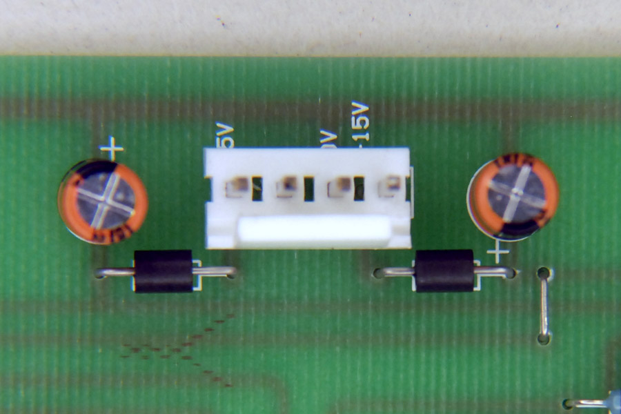
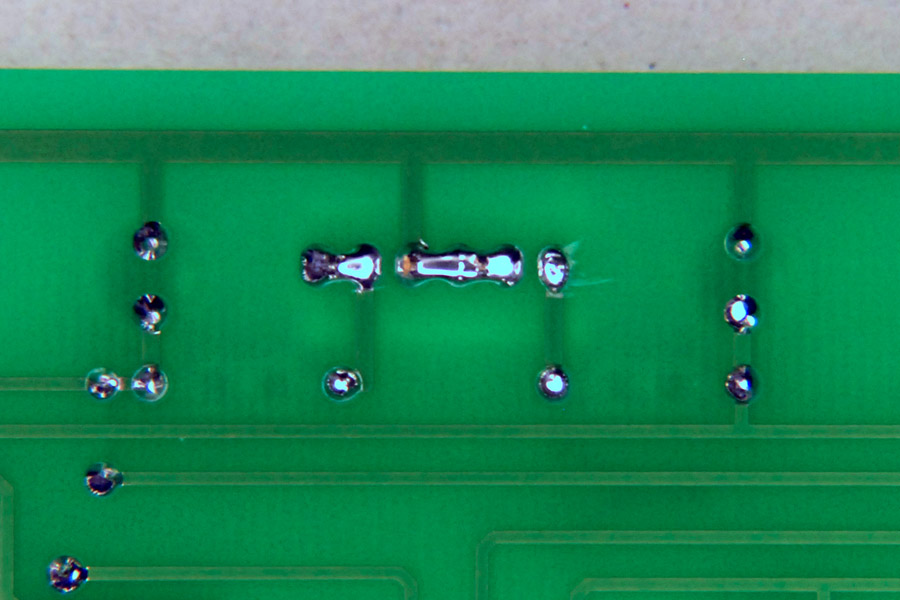
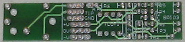
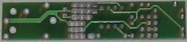
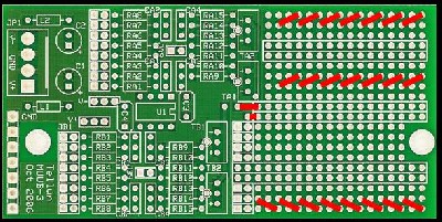
We've decided to provide separate jacks for each of the 22 band-pass outputs and the high and low pass outputs (we already have a "DRY OUT" jack). Scott Juskiw suggested we accomplish this by running leads from each pot on the pre-attenuator side to the corresponding jack. The effect will be that the signal at each individual output jack will be full-on. He pointed out that this way if we want to exclude that band from the mix at the "ALL CELLS" output jack, we can just turn its pot full-off. We like this. Now, you could put the jacks post-attenuator... but... We'll want to put an inverter/buffer in-line with each individual out jack. For this, we've decided to use the little Bridechamber / Ken Stone individual buffer pcbs - one on each jack. Here' the little PCB front and back:
Although they have a place for a little 3 pin power header, they don't have the typical power-supply capacitor / ferrite beads set-up. So we're going to use an MUUB3 for that part - it has contacts where we can solder leads to supply power to the little buffers. OK - it seems kind-of a waste - there's room on there for a couple buffers - but we're going to bypass these and just use the MUUB3 for power supply. |
||||||||||||||||||||||||||||||||||||||||||||||||||||||||||||||||||||||||||||||||||||||||||||||||||||||||||||||||||||||||||||||||||||||||||||||||||||||||||||||||||||||||||||||||||||||||||||||||||||||||||||||||||||||||
|
7A. Buffer / Inverter |
||||||||||||||||||||||||||||||||||||||||||||||||||||||||||||||||||||||||||||||||||||||||||||||||||||||||||||||||||||||||||||||||||||||||||||||||||||||||||||||||||||||||||||||||||||||||||||||||||||||||||||||||||||||||
|
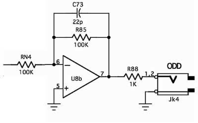
Looking at Yves' FFB schematic, here's what the output buffer should look like:
This can be accomplished by configuring the Bridechamber / Ken Stone pcb as follows:
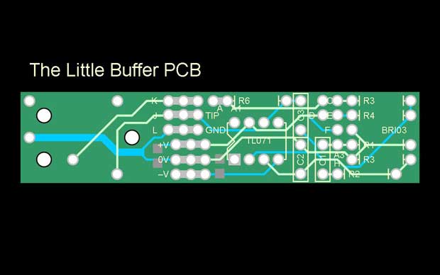
Here's how we idiots figured this out... (we're including this detail to show fellow idiots that by digging in and thinking about this stuff and figuring it out... well - it works - and if we can do it, believe us - you can too) So we took a really close look at the buffer PCB and we even charted it out like this (if you click on the image, you can download our PPT file complete with the "layers" or "groups" separated out - maybe you'll find it useful for your own applications - and if you click here, you can get to a page with our detailed images on it):
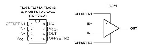
Then, we looked up the specs on the TL071 chip:
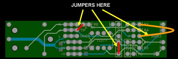
First thing we thought about was how to make the connections to the TL071 match Yves' output buffer schematic. We could see we'd have to connect the "IN+" pin (pin #3) of the TL071 to ground. We did that with the jumper at "C2." Next we thought about the output - that's pin #6. We figured out that we could put the 1K resistor at "R6" and then a jumper from it's left side to the "TIP" lead. OK - so now - TL071 input - the "IN-" pin (pin #2) well, we've got to feed that through a 100K resistor. So if we put the resistor at "R4" and the input goes to the pad just to it's left we figure we're in like Flynn. But we still have to accomplish the 22p Cap and 100K Resistor connections. It looks like that can be done across the "C3" place on the PCB. We want to accomplish a nice MTA-header connection for power and input... and taking all this into account illustrating it in detail - Here's where the jumpers go (if you right-click on these images, you'll get a bigger one to look at):
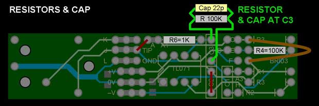
The resistors and the 22p cap:
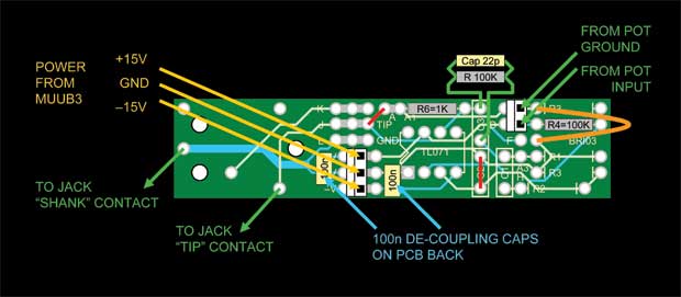
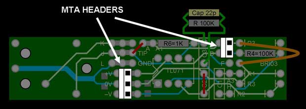
Here's where the MTA headers go:
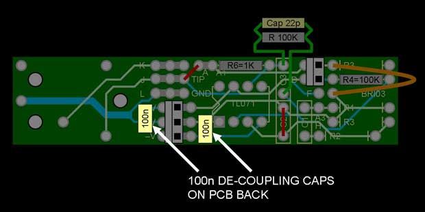
The de-coupling caps on the back:
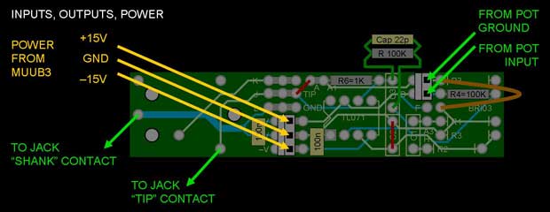
And the inputs, outputs, and power supply:
|
||||||||||||||||||||||||||||||||||||||||||||||||||||||||||||||||||||||||||||||||||||||||||||||||||||||||||||||||||||||||||||||||||||||||||||||||||||||||||||||||||||||||||||||||||||||||||||||||||||||||||||||||||||||||
|
7B. MUUB3 - Power Supply to Buffers |
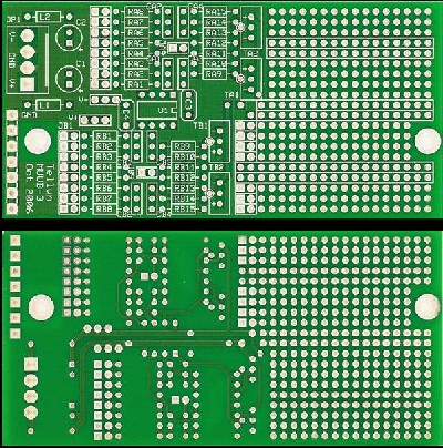
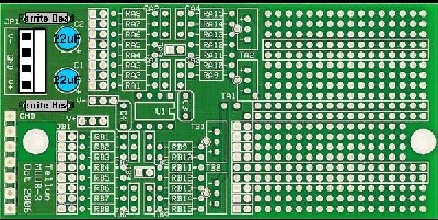
Here's how we'll configure the MUUB3s to supply power to the little buffers - here's what the MUUB3 PCBs look like (front and back):
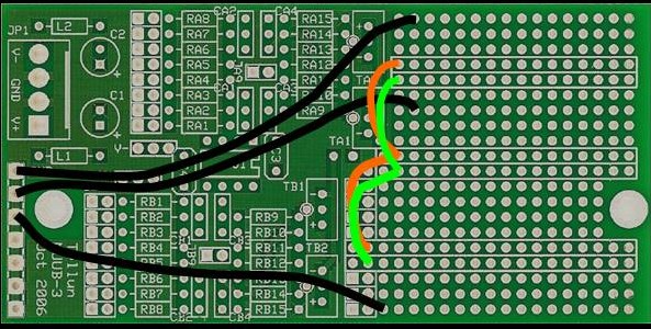
Here's how the power supply (to the MUUB3) will be built:
And here is how the whole MUUB3 pcb is laid out (click on the image to see a .pdf image):
To make it easier to see, Jumpers go here:
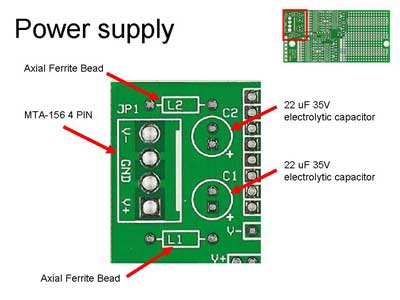
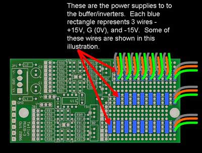
Power elements go here:
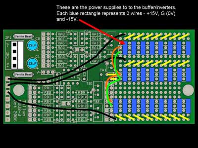
The positive and negative output power busses get wired up like this:
Here's the power outputs (click on the image to see a .pdf image):
|
|||||||||||||||||||||||||||||||||||||||||||||||||||||||||||||||||||||||||||||||||||||||||||||||||||||||||||||||||||||||||||||||||||||||||||||||||||||||||||||||||||||||||||||||||||||||||||||||||||||||||||||||||||||||
|
8. Bypass Switch/ Indicator LED Modification |
||||||||||||||||||||||||||||||||||||||||||||||||||||||||||||||||||||||||||||||||||||||||||||||||||||||||||||||||||||||||||||||||||||||||||||||||||||||||||||||||||||||||||||||||||||||||||||||||||||||||||||||||||||||||
|
The Grand Design... |
||||||||||||||||||||||||||||||||||||||||||||||||||||||||||||||||||||||||||||||||||||||||||||||||||||||||||||||||||||||||||||||||||||||||||||||||||||||||||||||||||||||||||||||||||||||||||||||||||||||||||||||||||||||||
|
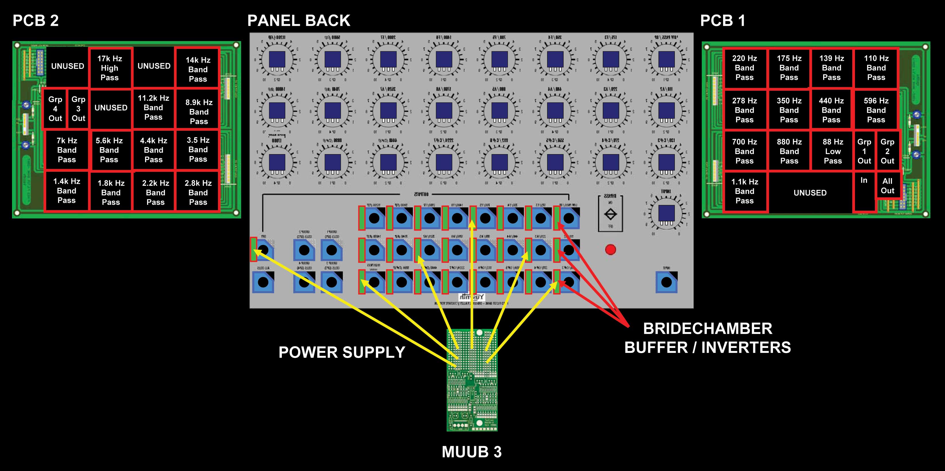
Lay-Out So - here is how these pieces are going to lay out (we'll deal with the exact mechanics and connections later):
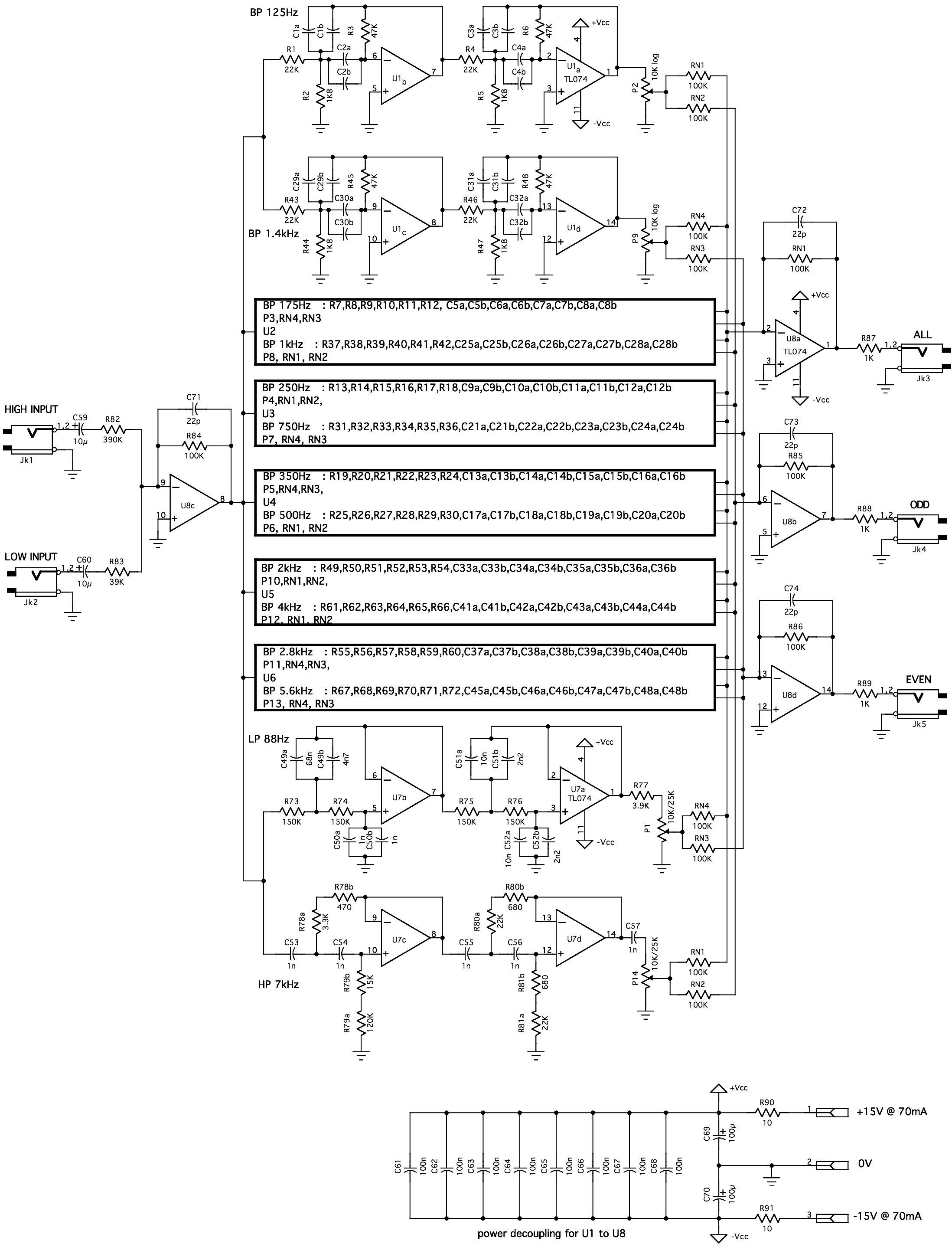
If you want a higher resolution picture, click here (450kb). OK - that's a cool diagram of the layout - but what are in its guts? Now - fellow idiots - just take a deep breath.... really - if we can do it you can too (non-idiots can just smile smugly). Yves (the infinitely gracious and very cool) went on to calculate the values of the band pass filters' resistors and capacitors to create our band frequencies. Here they are.
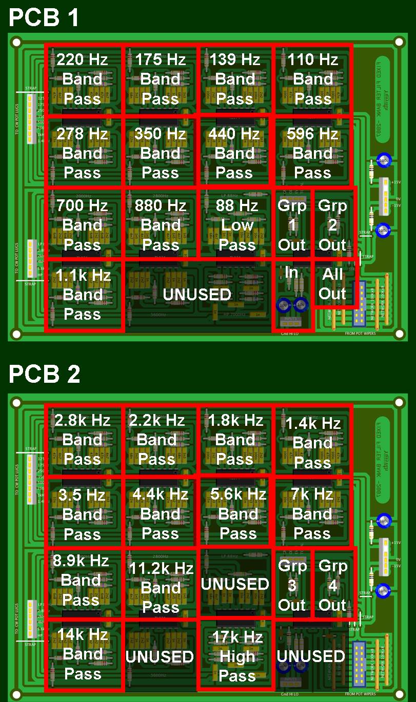
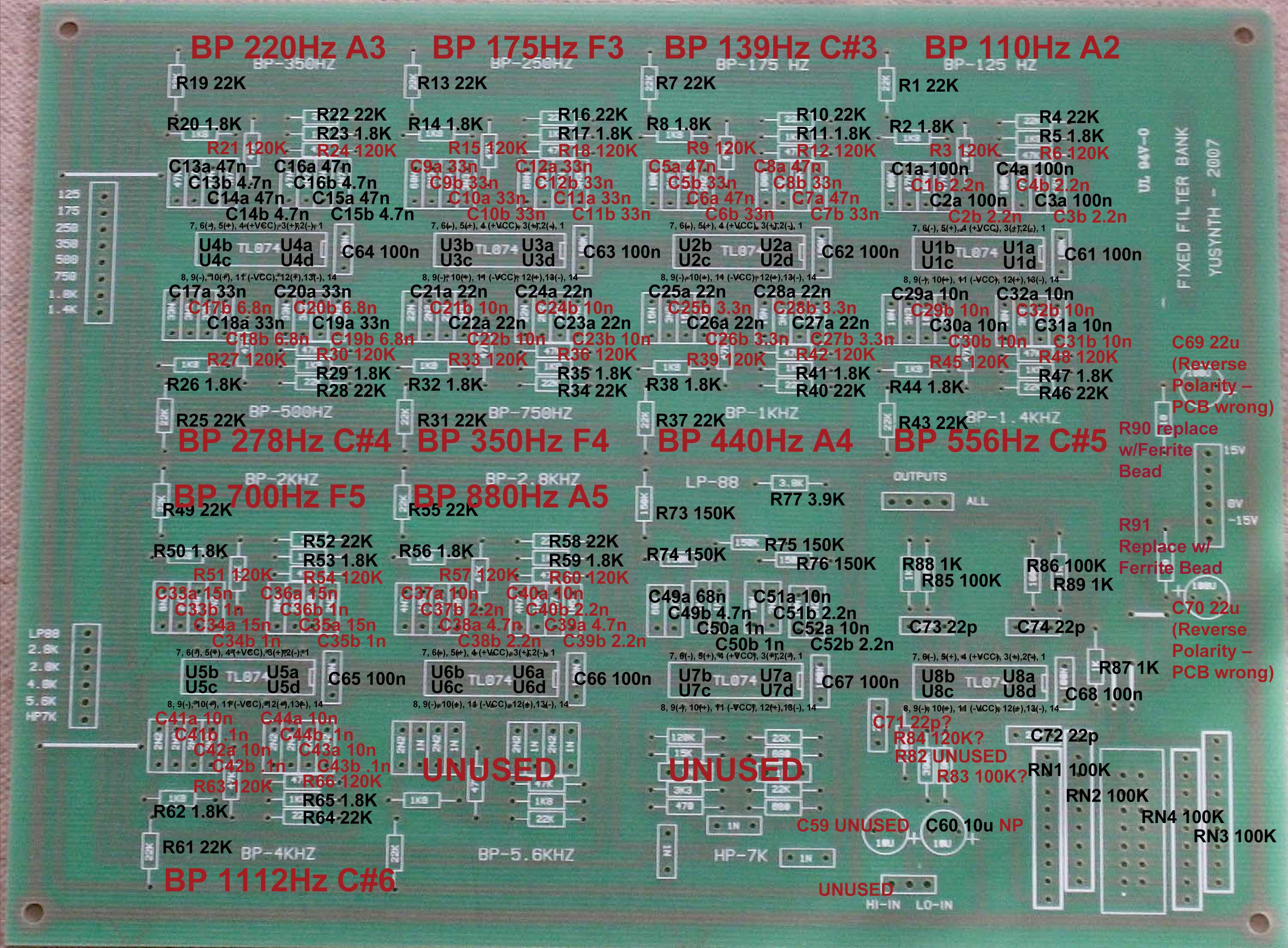
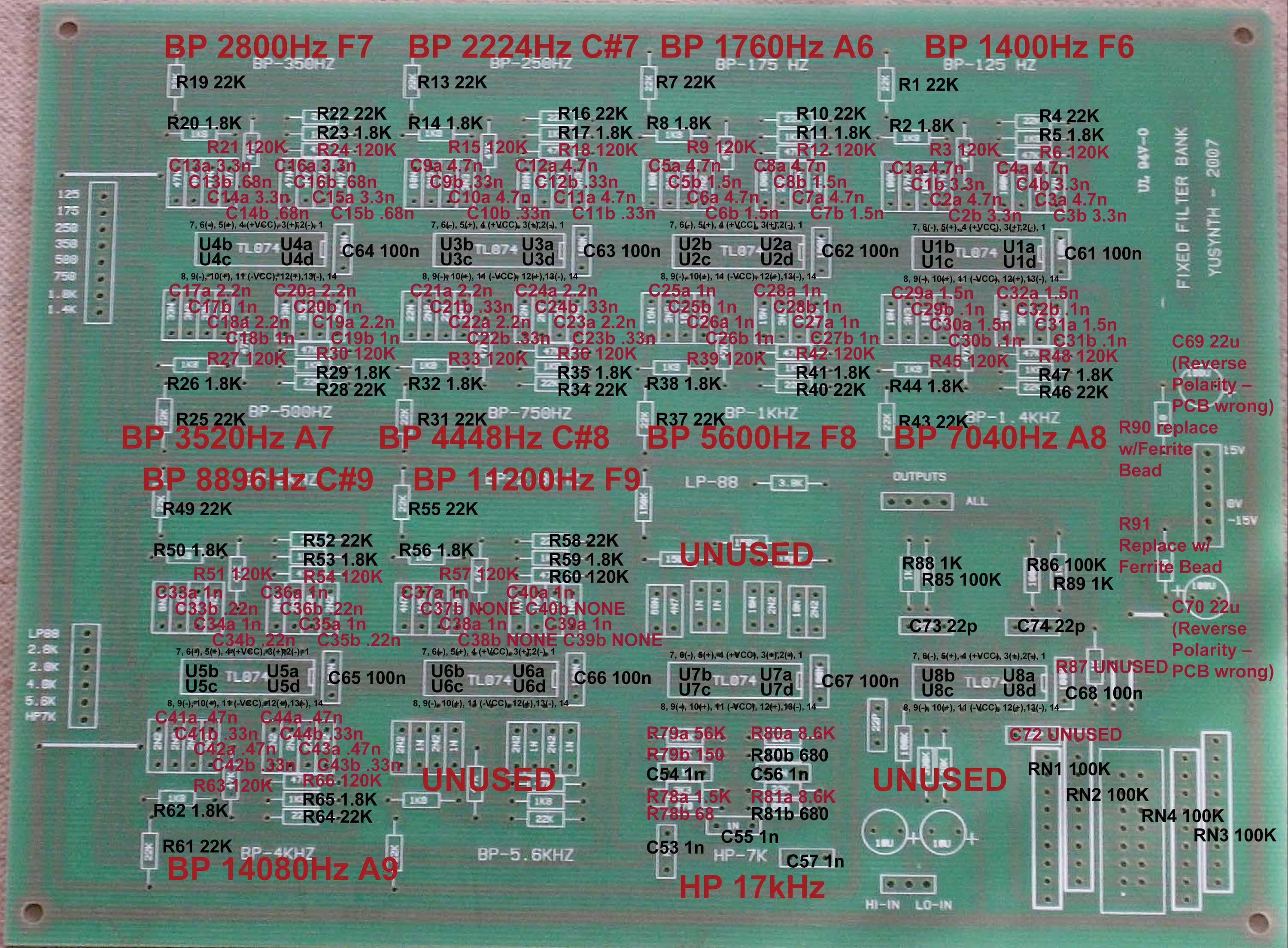
And he sent us these values for HP 17kHz: And he said to change the value of R84 to 12K We wondered about this - it seems such a drastic change from its former 100k value. So we asked Yves about it and he said: "Hi Bill and Will "No I really mean 12k for R84 ! No mistake there. Here is why : "In order to design 1/3 octave band-pass cells it was necessary to significantly increase their Q (resonance) but this has a consequence on their gain which in turn increases dramatically. Therefore, in order to avoid saturation and distortion in the BP cells, it is necessary to pre-attenuate the input signal. This why I selected a 12K resistor value for R84 which should compensate for the gain increase of the BP cells. "Obviously this value is a calculated value, I have not built this version of the FFB and it may be necessary that you adjust the value of R84 in such a way that the FFB has an overall gain of 1 when all the cells are fully cranked up. "Regards, Yves" Thanks again, Yves. YUSynth FFB PCB Specifications Right - great - so What The Frill does this mean? Remember that annotated PCB image we created way up on this page? (Click here) Right - well - here's why we did it. It was to help us figure out the locations of the parts and their quantities. Here are the images of the two PCBs showing Yves' new values for the filter resistors, capacitors, etc. PCB1:
Click here for a high-resolution jpeg version (890K) Click here for a high-resolution pdf version (250K) PCB2:
Click here for a high-resolution jpeg version (890K) Click here for a high-resolution pdf version (250K) But while we'd been over-heating our brains with all this thinking, it had snowed outside and it's time for a snack. Steak will do nicely - but Will declared "let's grill it!" hense - |
||||||||||||||||||||||||||||||||||||||||||||||||||||||||||||||||||||||||||||||||||||||||||||||||||||||||||||||||||||||||||||||||||||||||||||||||||||||||||||||||||||||||||||||||||||||||||||||||||||||||||||||||||||||||
|
|
||||||||||||||||||||||||||||||||||||||||||||||||||||||||||||||||||||||||||||||||||||||||||||||||||||||||||||||||||||||||||||||||||||||||||||||||||||||||||||||||||||||||||||||||||||||||||||||||||||||||||||||||||||||||
|
December 2007 - Parts |
||||||||||||||||||||||||||||||||||||||||||||||||||||||||||||||||||||||||||||||||||||||||||||||||||||||||||||||||||||||||||||||||||||||||||||||||||||||||||||||||||||||||||||||||||||||||||||||||||||||||||||||||||||||||
|
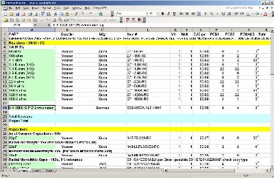
Will and I have developed a parts-list / bill-of-materials in the form of an XL spreadsheet (as usual). Yves has been very patient and helpful answering our many questions - and - yes, they have been pesky. We want to thank Dave Brown and mrmike as well concerning parts issues. As of today, 1 December 2007, it's virtually complete - but please don't take it as gospel. Even so, just now we've used it to make our Mouser purchases and we are relatively confident in our specifications. Note: Yves specified that R80a and R80b should be 8.6K. Well - mouser doesn't carry these. They are, however, in series and their total resistance is 9280 ohms. We can get around the problem by specifying R80a at 9.1K (9100) and R80b at 180 ohms - so that's what we did.
Click here to download our XL spreadsheet Parts List |
||||||||||||||||||||||||||||||||||||||||||||||||||||||||||||||||||||||||||||||||||||||||||||||||||||||||||||||||||||||||||||||||||||||||||||||||||||||||||||||||||||||||||||||||||||||||||||||||||||||||||||||||||||||||
Panel
For our FPD panel design, click here.
|
||||||||||||||||||||||||||||||||||||||||||||||||||||||||||||||||||||||||||||||||||||||||||||||||||||||||||||||||||||||||||||||||||||||||||||||||||||||||||||||||||||||||||||||||||||||||||||||||||||||||||||||||||||||||
Construction Phase 1All the stuff in Phase 1 gets soldered using "Organic" Solder. At every break in the action, we wash the board off to get rid of the flux. |
||||||||||||||||||||||||||||||||||||||||||||||||||||||||||||||||||||||||||||||||||||||||||||||||||||||||||||||||||||||||||||||||||||||||||||||||||||||||||||||||||||||||||||||||||||||||||||||||||||||||||||||||||||||||
Construction Phase 2All the stuff in Phase 2 gets soldered using "No-Clean" Solder and the PCB doesn't get washed off from here on. |
||||||||||||||||||||||||||||||||||||||||||||||||||||||||||||||||||||||||||||||||||||||||||||||||||||||||||||||||||||||||||||||||||||||||||||||||||||||||||||||||||||||||||||||||||||||||||||||||||||||||||||||||||||||||
Set up / Testing |
||||||||||||||||||||||||||||||||||||||||||||||||||||||||||||||||||||||||||||||||||||||||||||||||||||||||||||||||||||||||||||||||||||||||||||||||||||||||||||||||||||||||||||||||||||||||||||||||||||||||||||||||||||||||
Use Notes |
||||||||||||||||||||||||||||||||||||||||||||||||||||||||||||||||||||||||||||||||||||||||||||||||||||||||||||||||||||||||||||||||||||||||||||||||||||||||||||||||||||||||||||||||||||||||||||||||||||||||||||||||||||||||
|
|
||||||||||||||||||||||||||||||||||||||||||||||||||||||||||||||||||||||||||||||||||||||||||||||||||||||||||||||||||||||||||||||||||||||||||||||||||||||||||||||||||||||||||||||||||||||||||||||||||||||||||||||||||||||||
)
)
)


|
The fine Print: Use this site at your own risk. We are self-proclaimed idiots and any use of this site and any materials presented herein should be taken with a grain of Kosher salt. If the info is useful - more's the better. Bill and Will © 2005-2011 all frilling rights reserved
|