Bill and Will's Synth
|
|
Table of Contents |
|
|
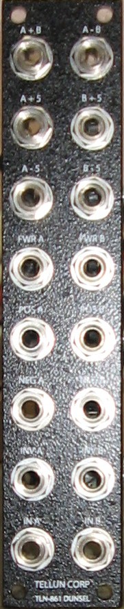
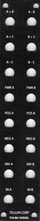
This process has become so long that we've broken it into three separate pages and sections within them. Here's a table of contents that we hope will make it easier to traverse them: Background - presents an explanation and Scott Juskiw's initial description of the module with a photo Parts - presents a Bill of Materials and notes about it Panel - presents the MOTM format panel Mounting Brackets - our use of two "Stooge" 3-pot brackets MUUB Construction Page (this Page) Construction PCB 1A&B - MUUB4 Construction PCB 2A&B - MUUB4 Construction PCB 3A&B - MUUB2 Construction PCB 4 - MUUB2 PCB Connections - wiring the PCBs together Panel Wiring - connecting the PCBs to the panel |
|
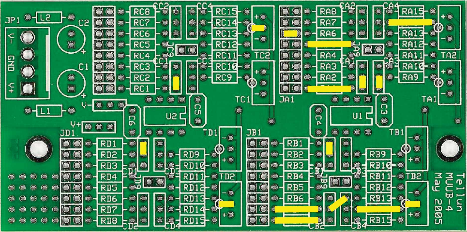
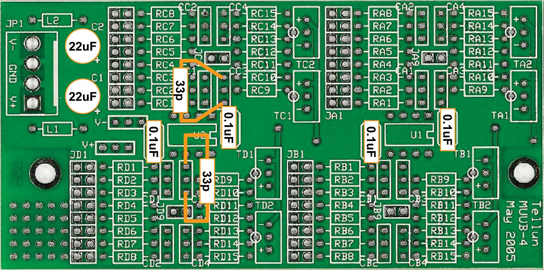
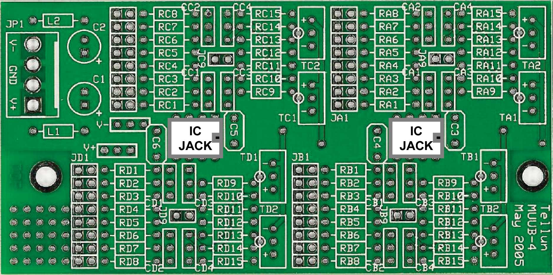
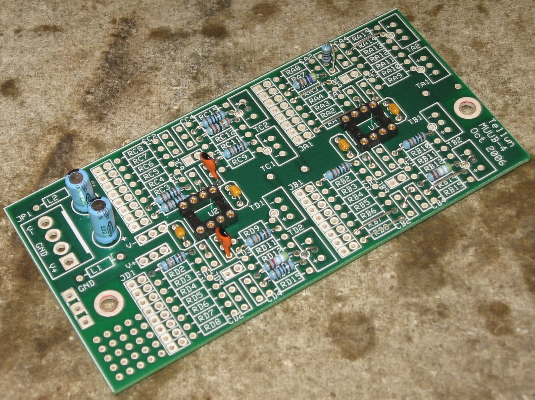
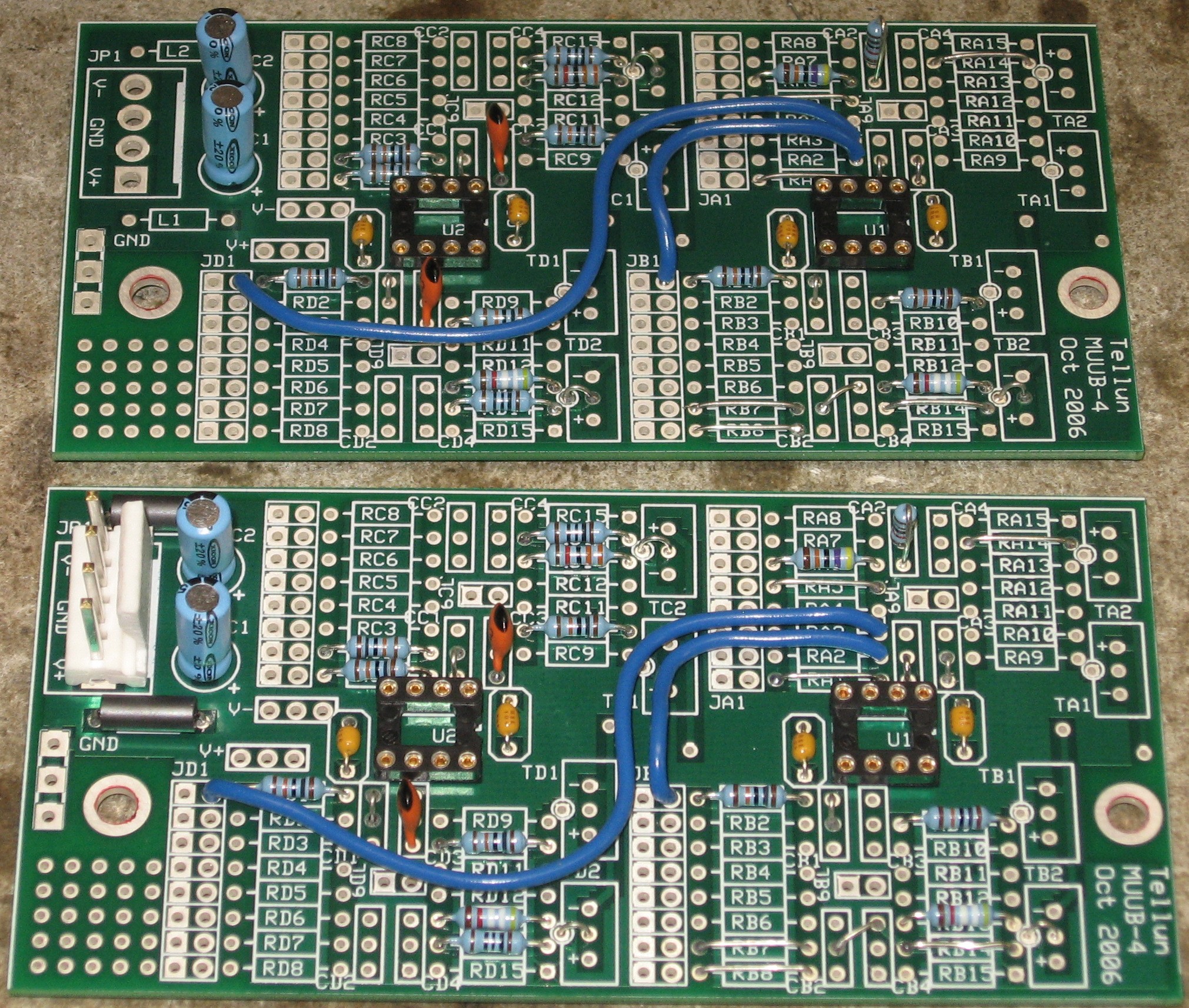
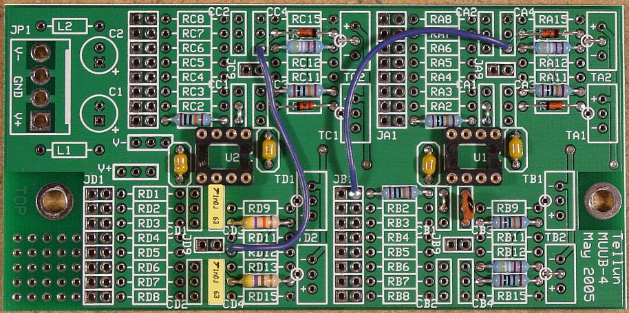
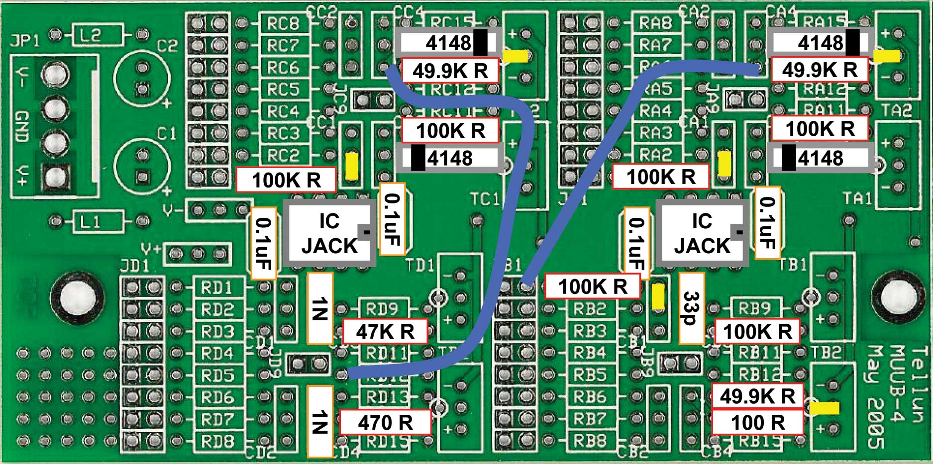
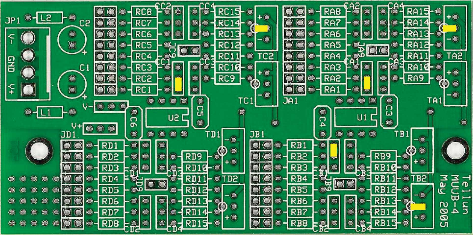
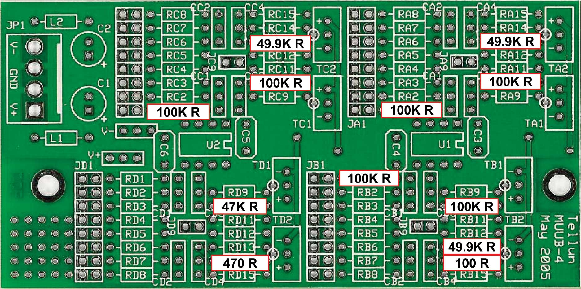
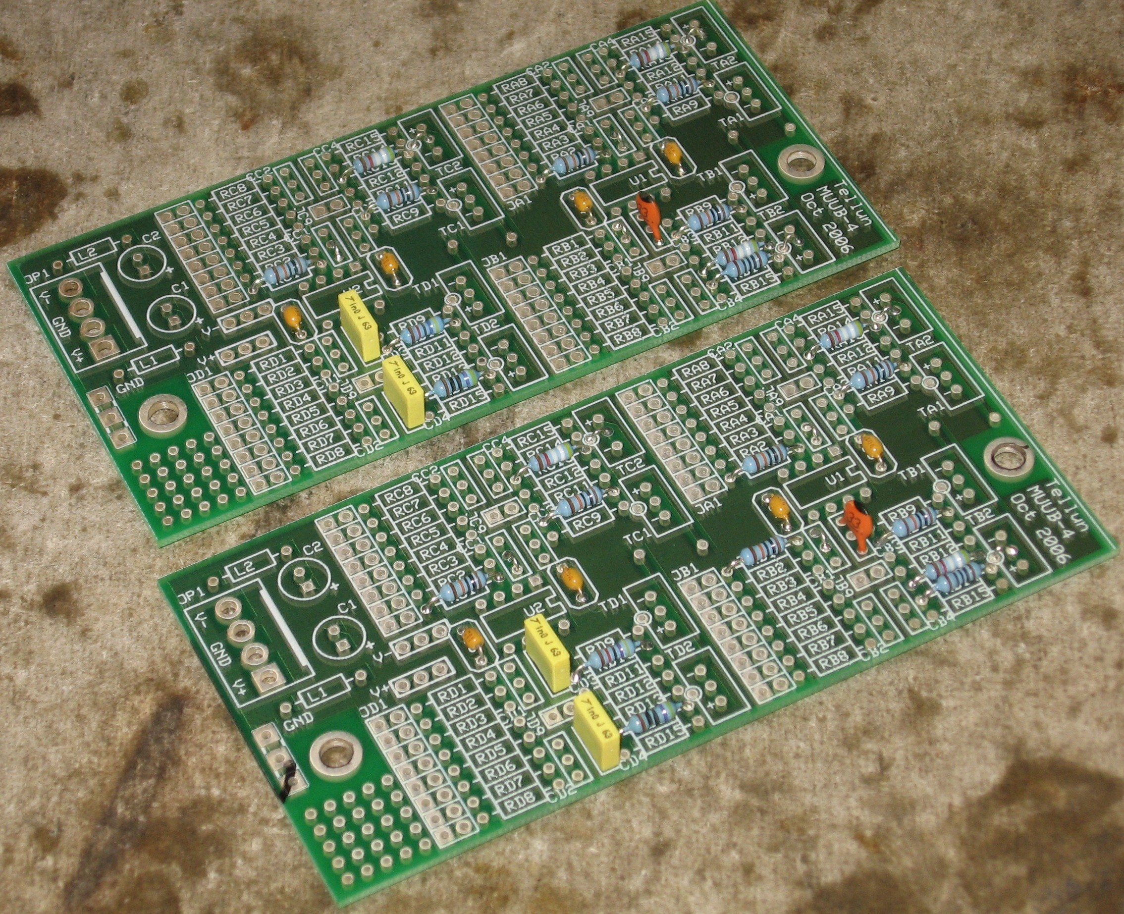
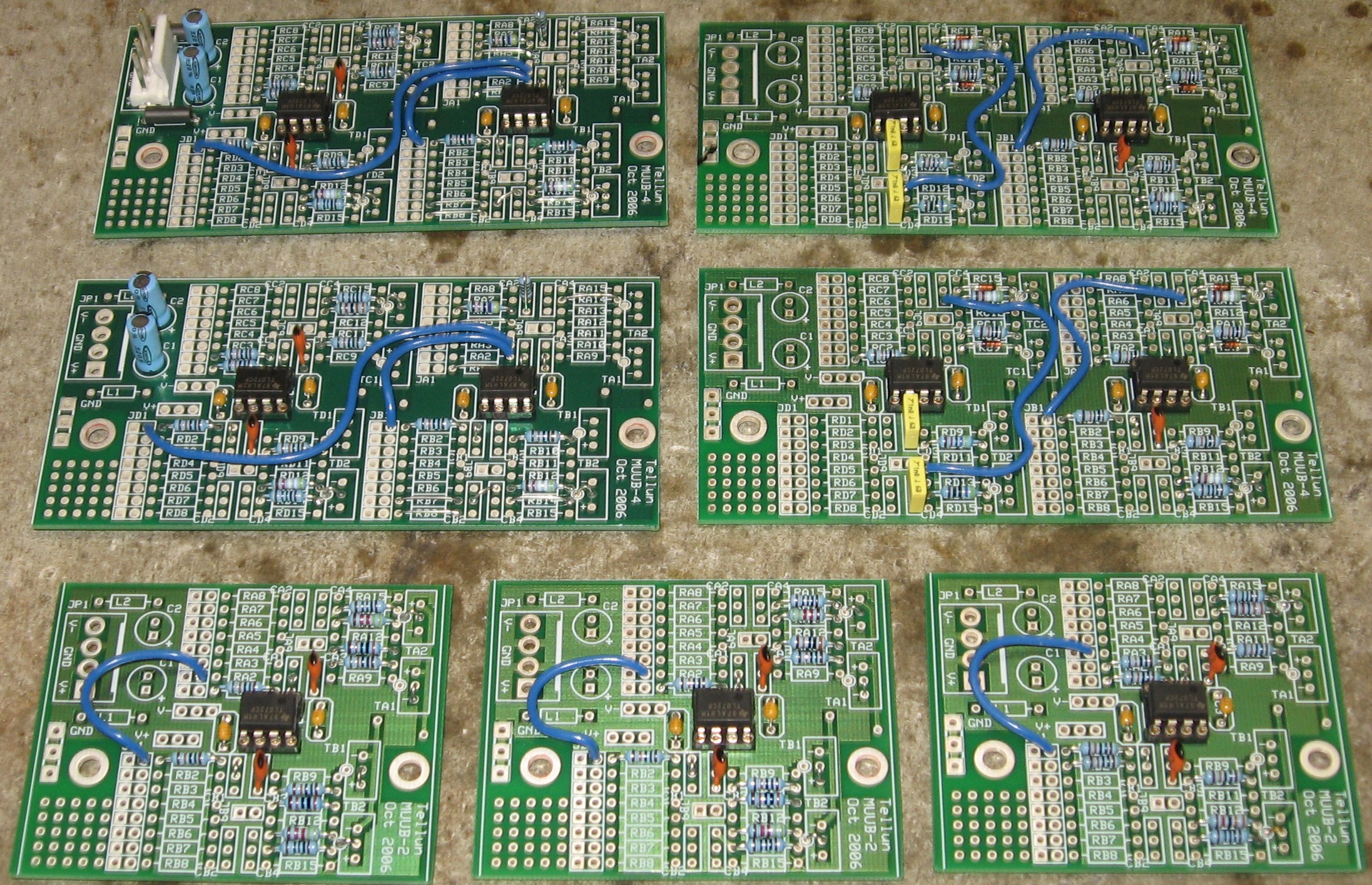
Construction - PCB1 A & BPCB1 A & B are built using MUUB4s and are described in Scott's 861 User's guide section 5.1. and 5.2. For detailed drawings of the MUUB4, click here. Please note again that during our build of these boards we discovered the omission of the JA6 jumper from the User Guide. That jumper is included in our diagrams, noted where relevant, and, after we discovered it, shown in our build photos. The two boards are identical except for the power elements so we're going to build them together.
Here's Scott's picture of Board A finished:
And his picture of Board B finished:
|
|
Phase 1All the stuff in Phase 1 gets soldered using "Organic" Solder. At every break in the action, we wash the board off to get rid of the flux. |
|
Jumpers |
|
|
|
|
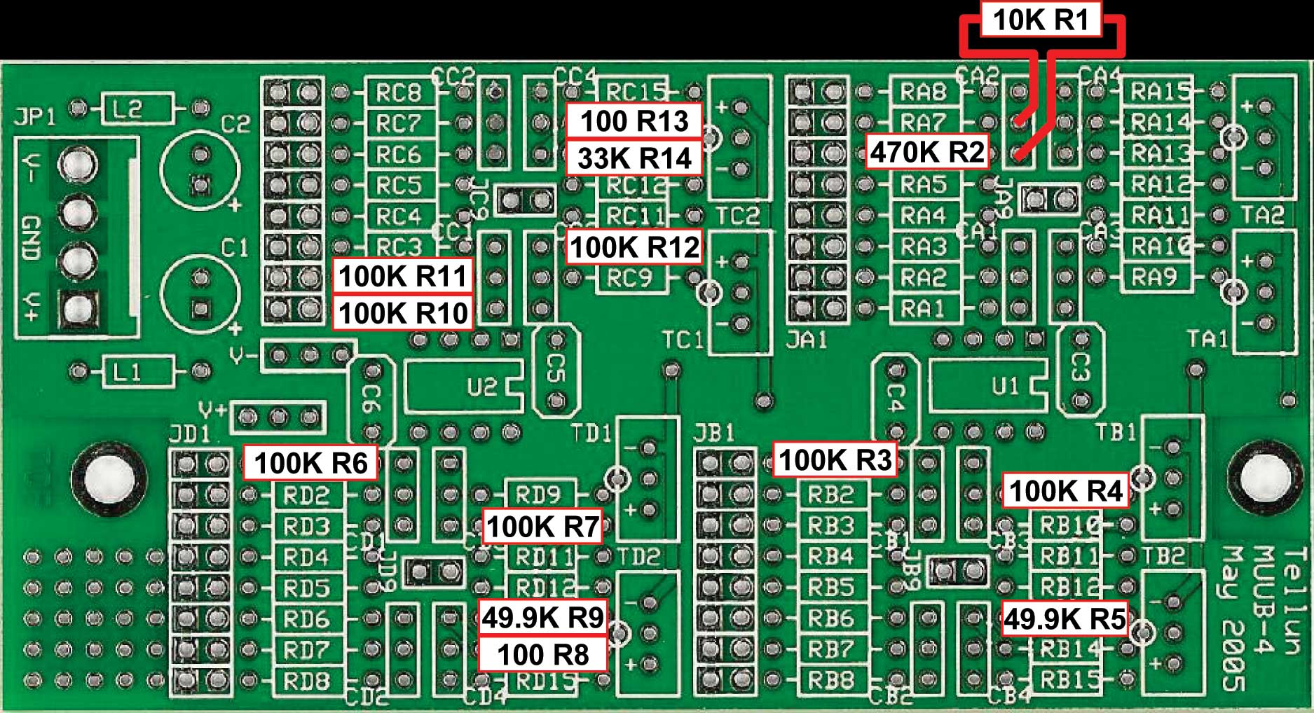
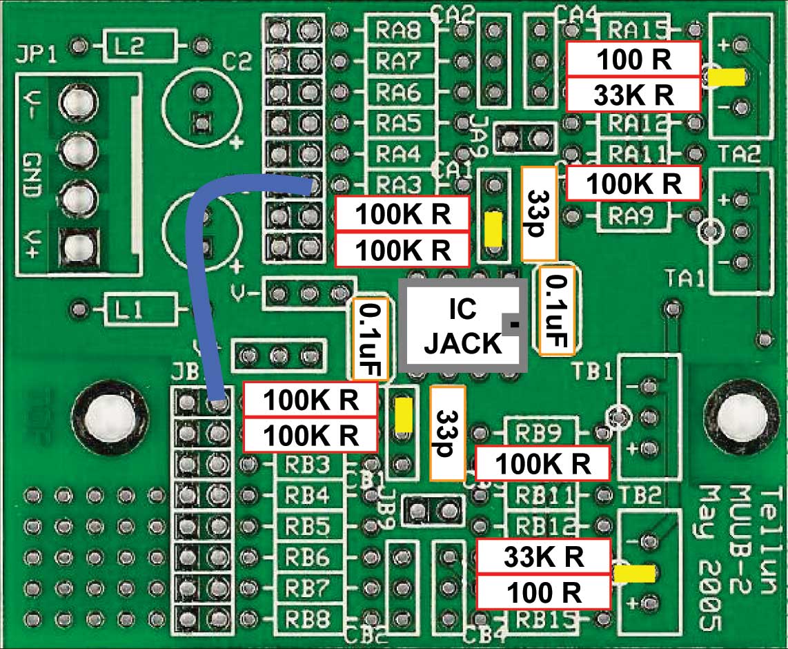
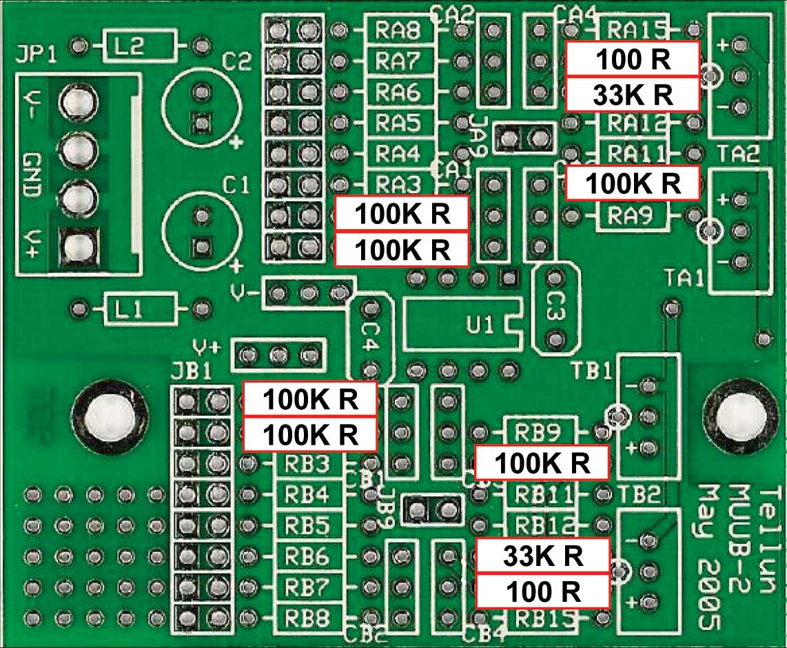
Resistors |
|
|
|
|
Capacitors |
|
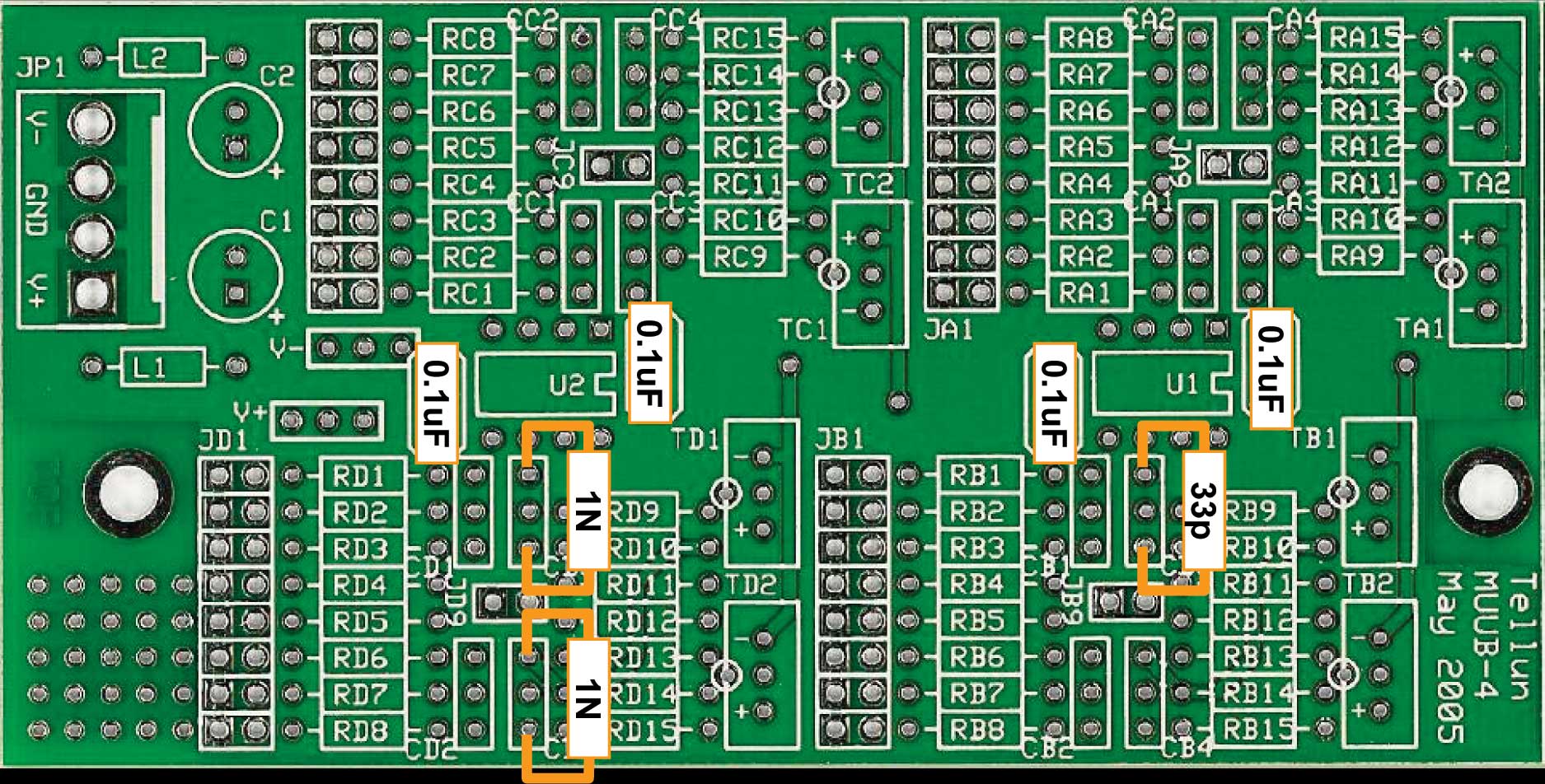
Misc |
Misc stuff for PCB 1 A
Misc stuff for PCB 1 B
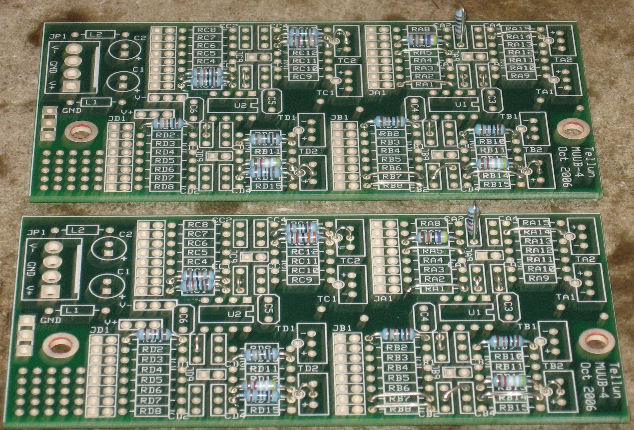
We're going to wash off the PCB at this point and let it dry.
We're going to wash off the PCB at this point and let it dry. |
Phase 2The stuff in Phase 2 gets soldered using "No-Clean" Solder and the PCB doesn't get washed off from here on. |
|
Wire jumpers |
|
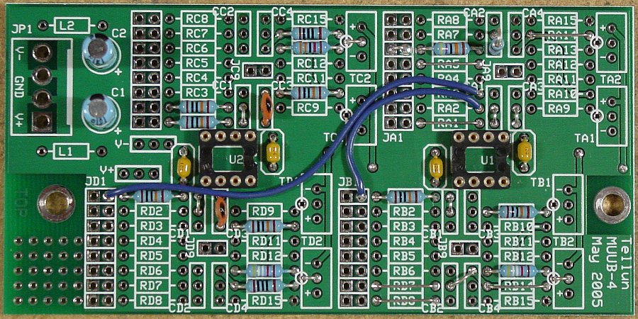
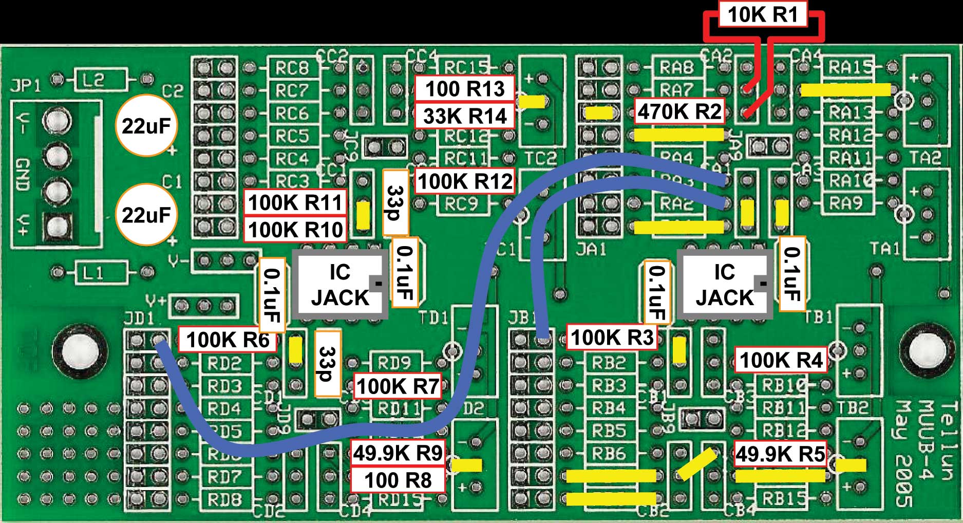
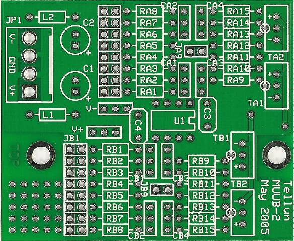
Construction - PCB2 A & BPCB 2 A & B are built using MUUB4s and are described in Scott's 861 User's guide section 5.3. and 5.3. The two boards are identical so we're going to build them together. Here's Scott's picture of Board A finished:
|
|
Phase 1Again, all the stuff in Phase 1 gets soldered using "Organic" Solder. At every break in the action, we wash the board off to get rid of the flux. |
|
Jumpers |
|
|
|
|
Resistors |
|
|
|
|
Capacitors |
|
Misc |
We're going to wash off the PCB at this point and let it dry. |
|
Phase 2 The stuff in Phase 2 gets soldered using "No-Clean" Solder and the PCB doesn't get washed off from here on. |
|
|
Wire jumpers |
|
|
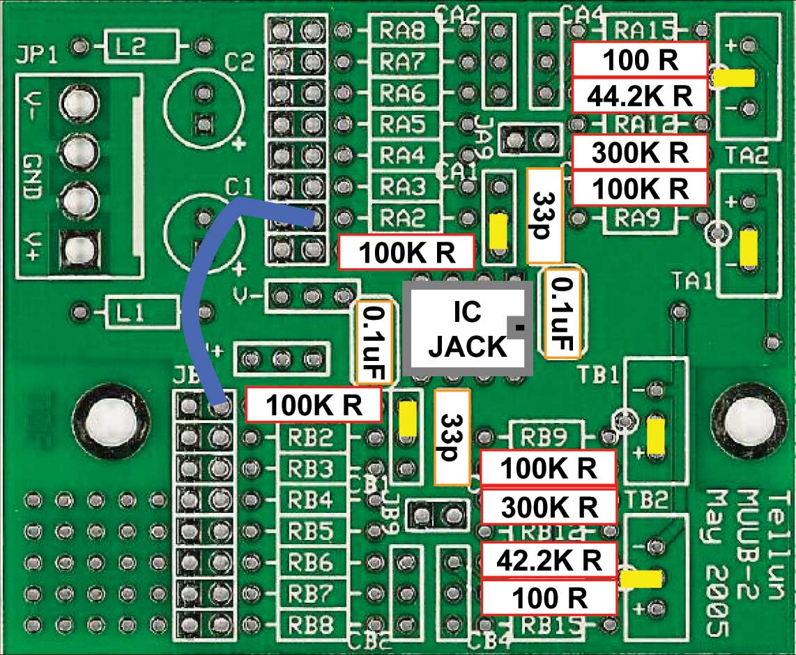
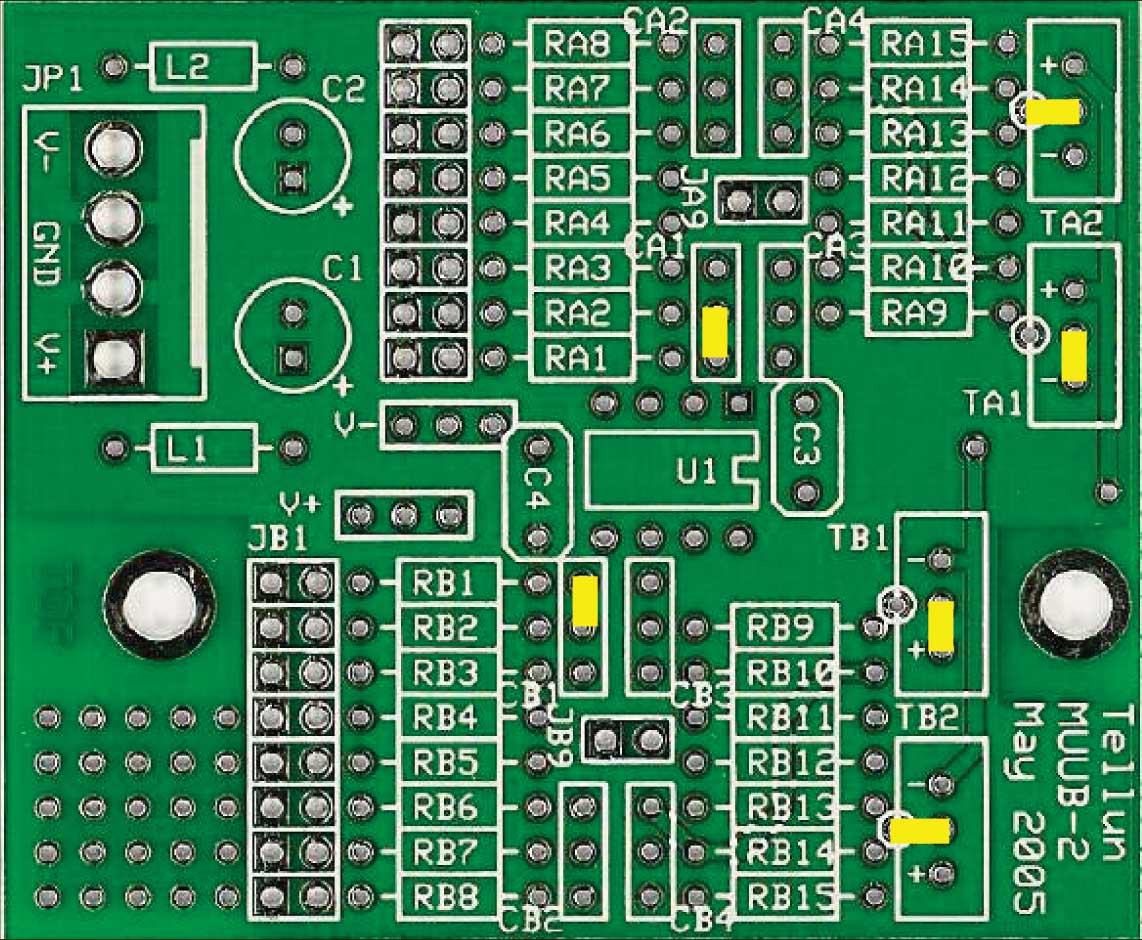
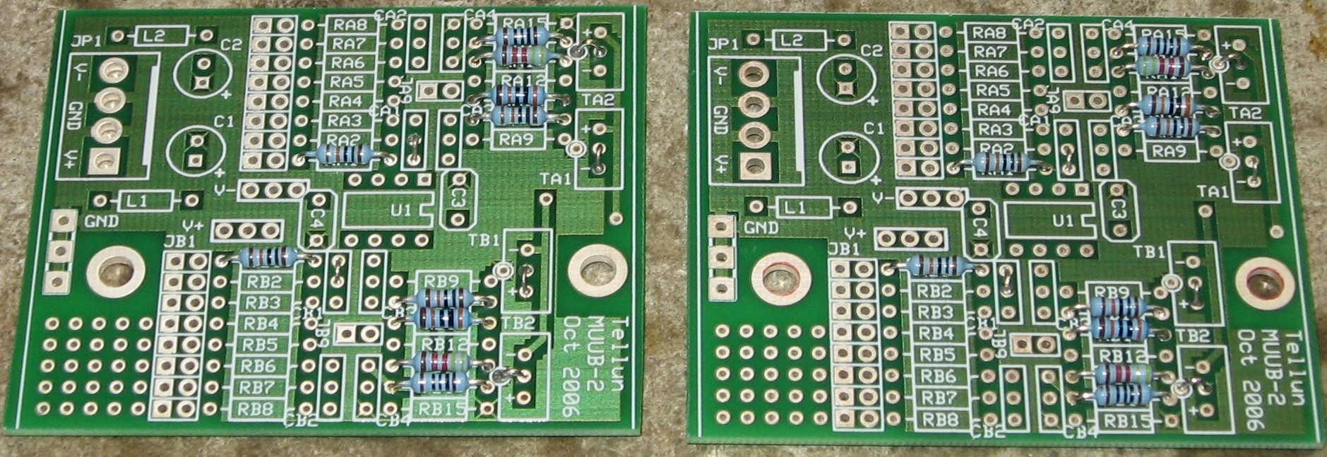
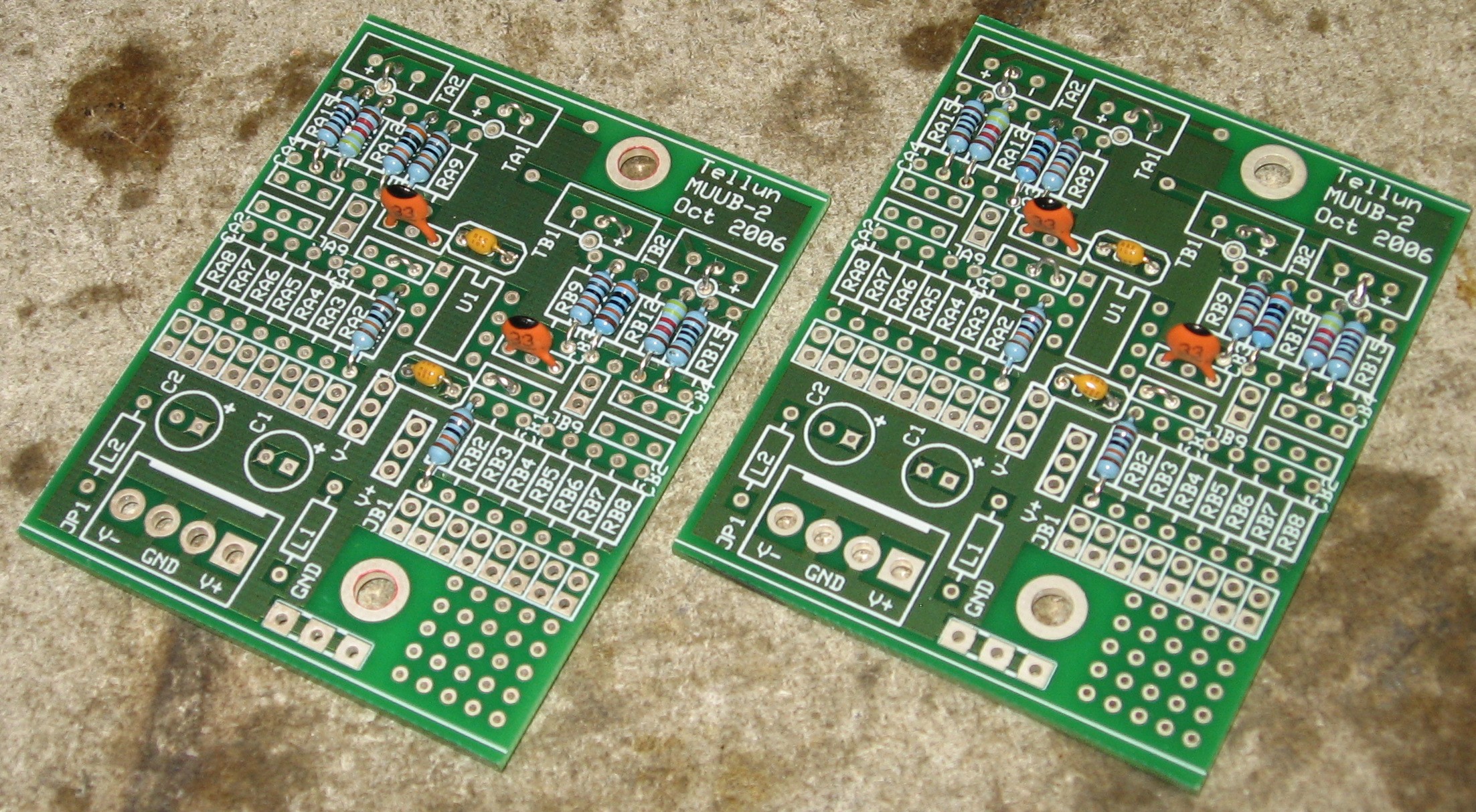
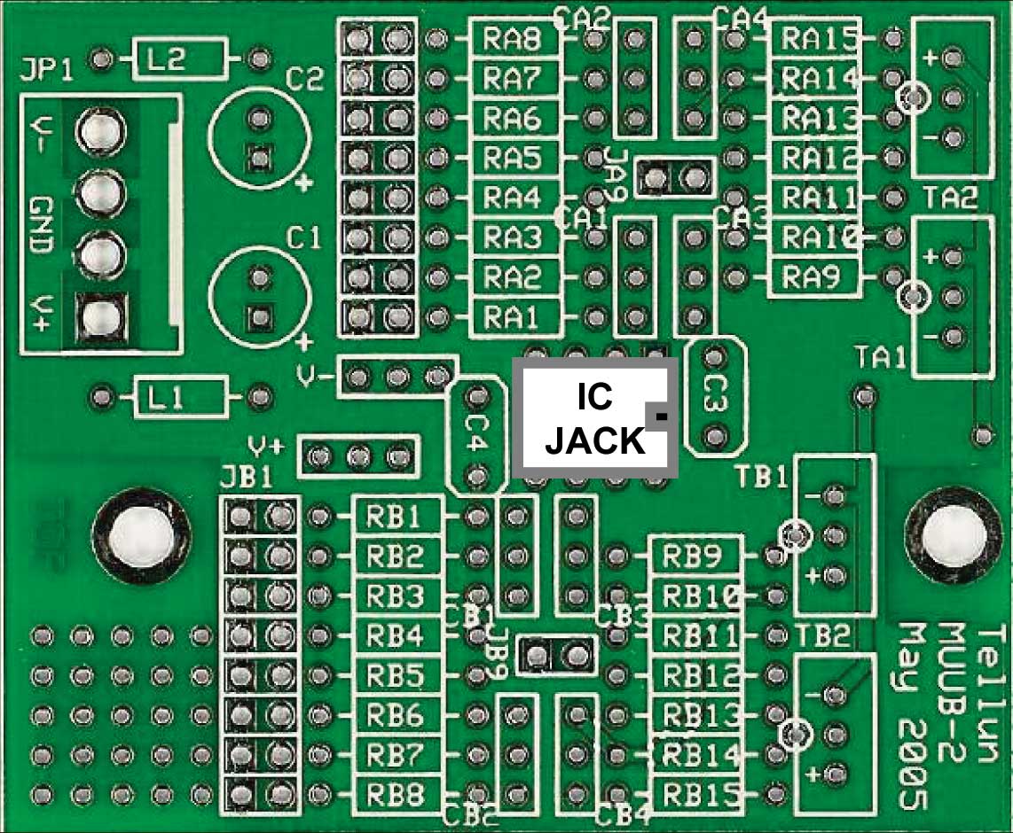
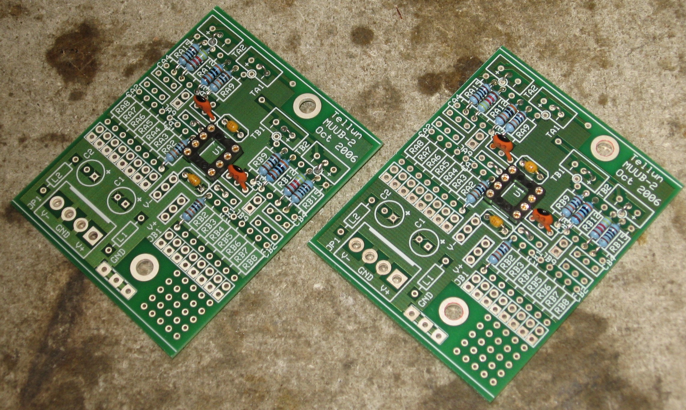
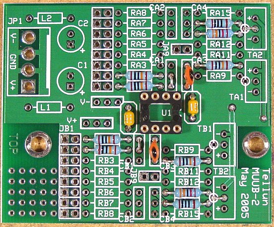
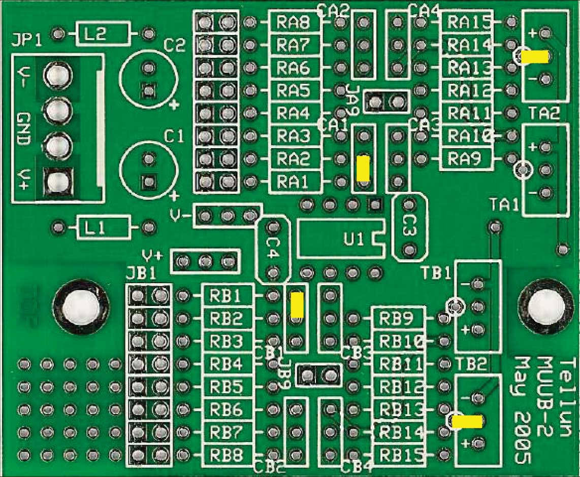
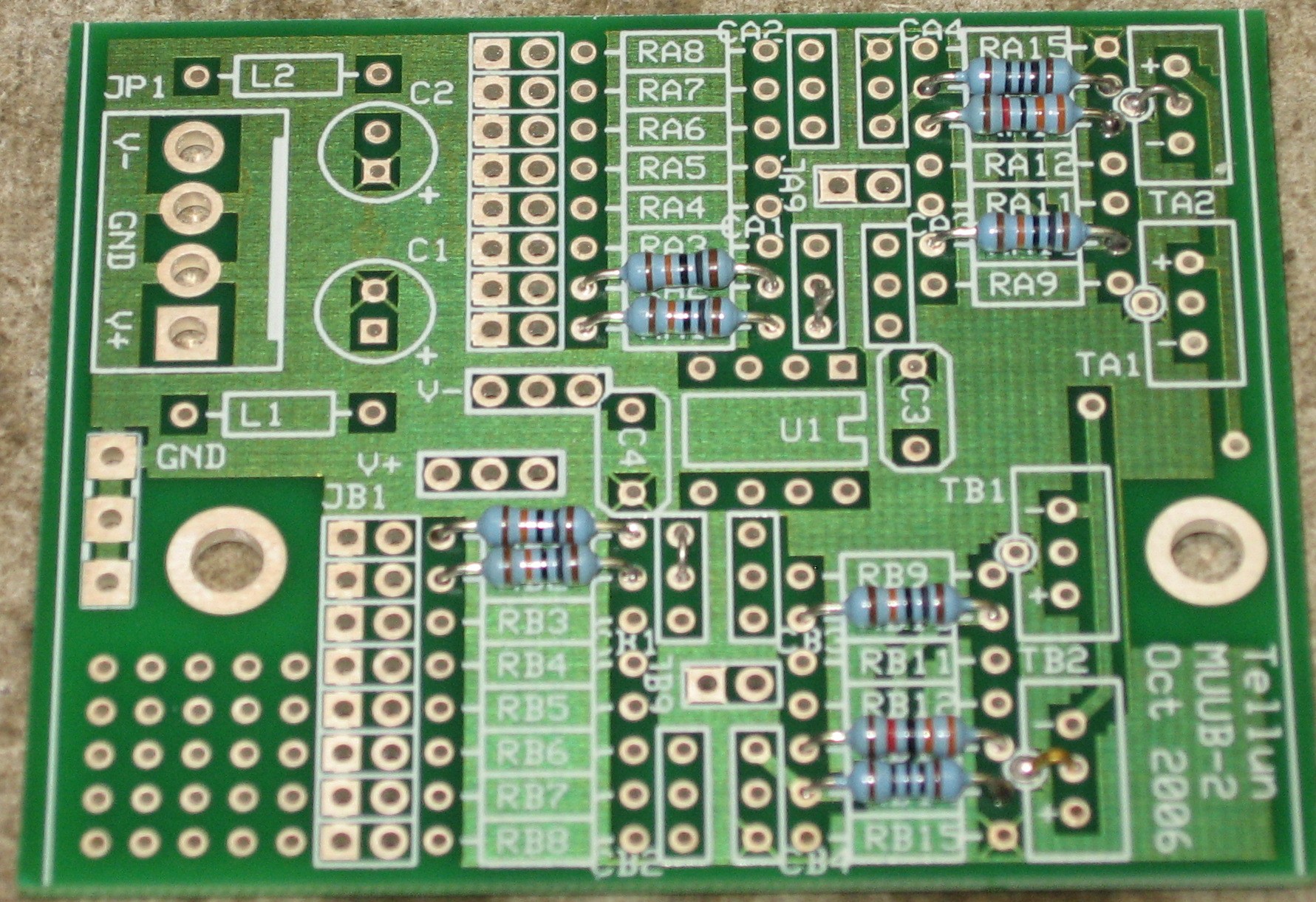
Construction - PCB3 A & B PCB3 A & B are built using MUUB2s and are described in Scott's 861 User's guide section 5.5. and 5.6. For detailed drawings of the MUUB2, click here.
The two boards are identical so we're going to build them together. Here's Scott's picture of Board A finished:
|
|
|
Phase 1 All the stuff in Phase 1 gets soldered using "Organic" Solder. At every break in the action, we wash the board off to get rid of the flux. |
|
|
Jumpers |
|
|
|
|
|
Resistors |
|
|
|
|
|
Capacitors |
|
|
Misc |
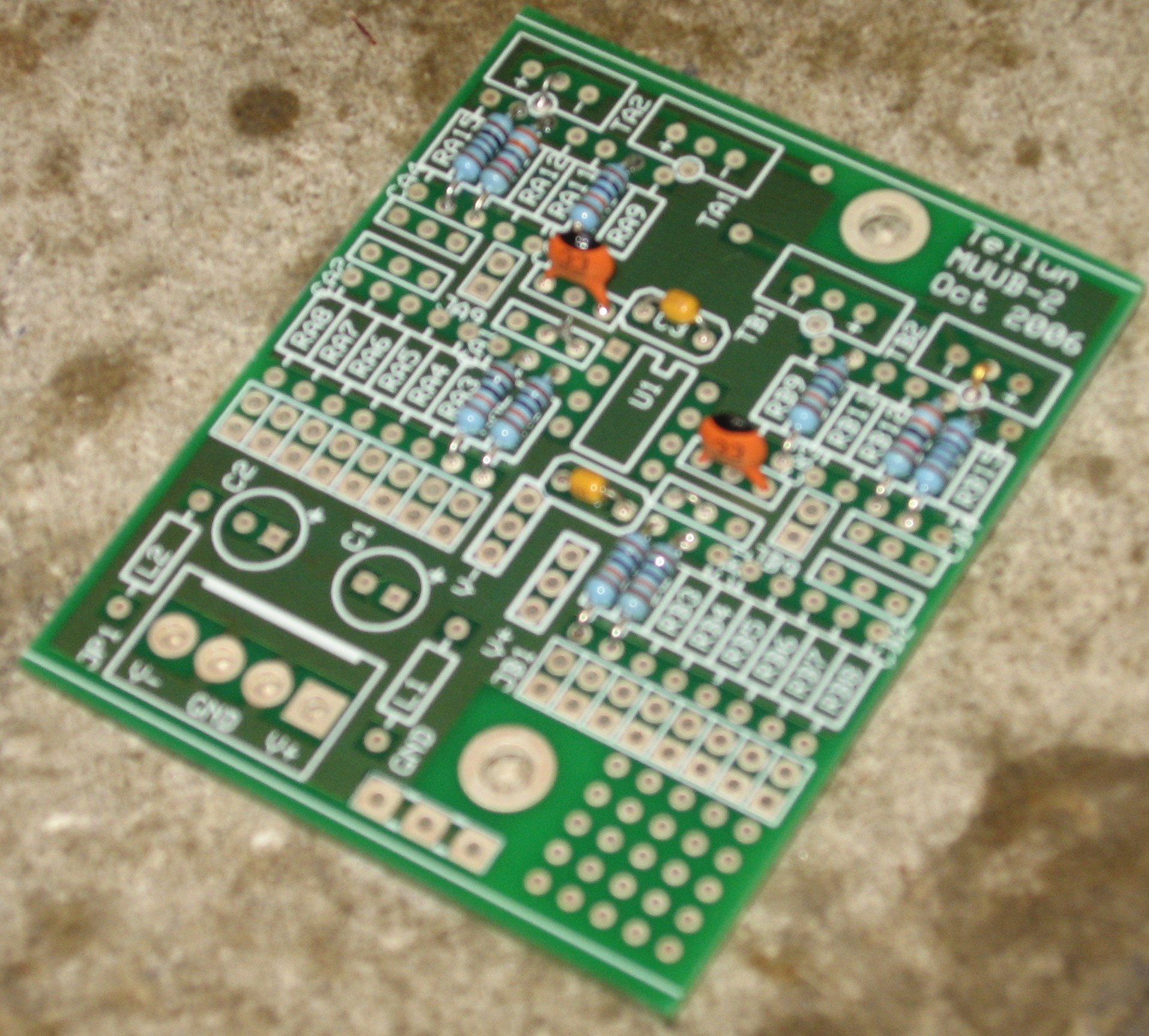
Misc stuff for PCB3 A & B
We're going to wash off the PCB at this point and let it dry. |
|
Phase 2 The stuff in Phase 2 gets soldered using "No-Clean" Solder and the PCB doesn't get washed off from here on. |
|
|
Wire jumpers |
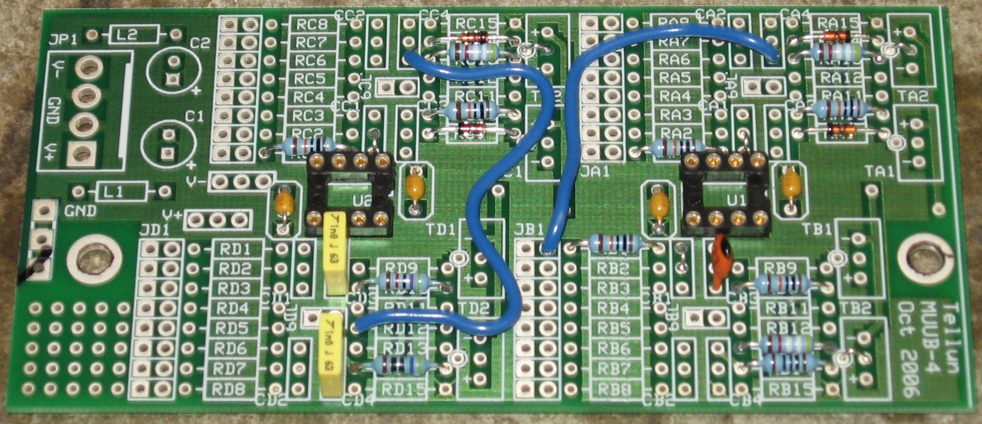
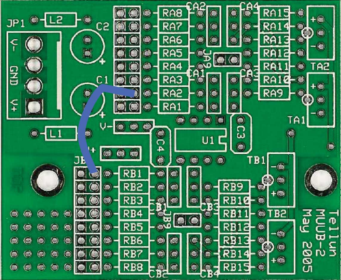
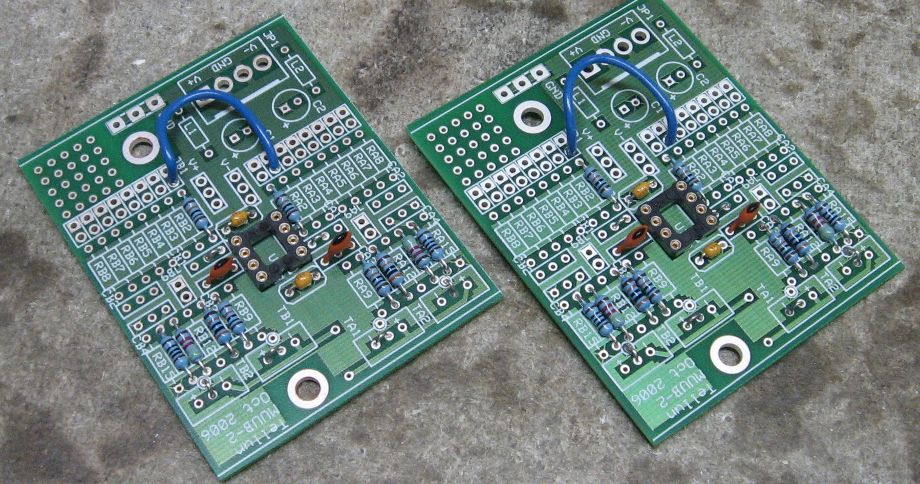
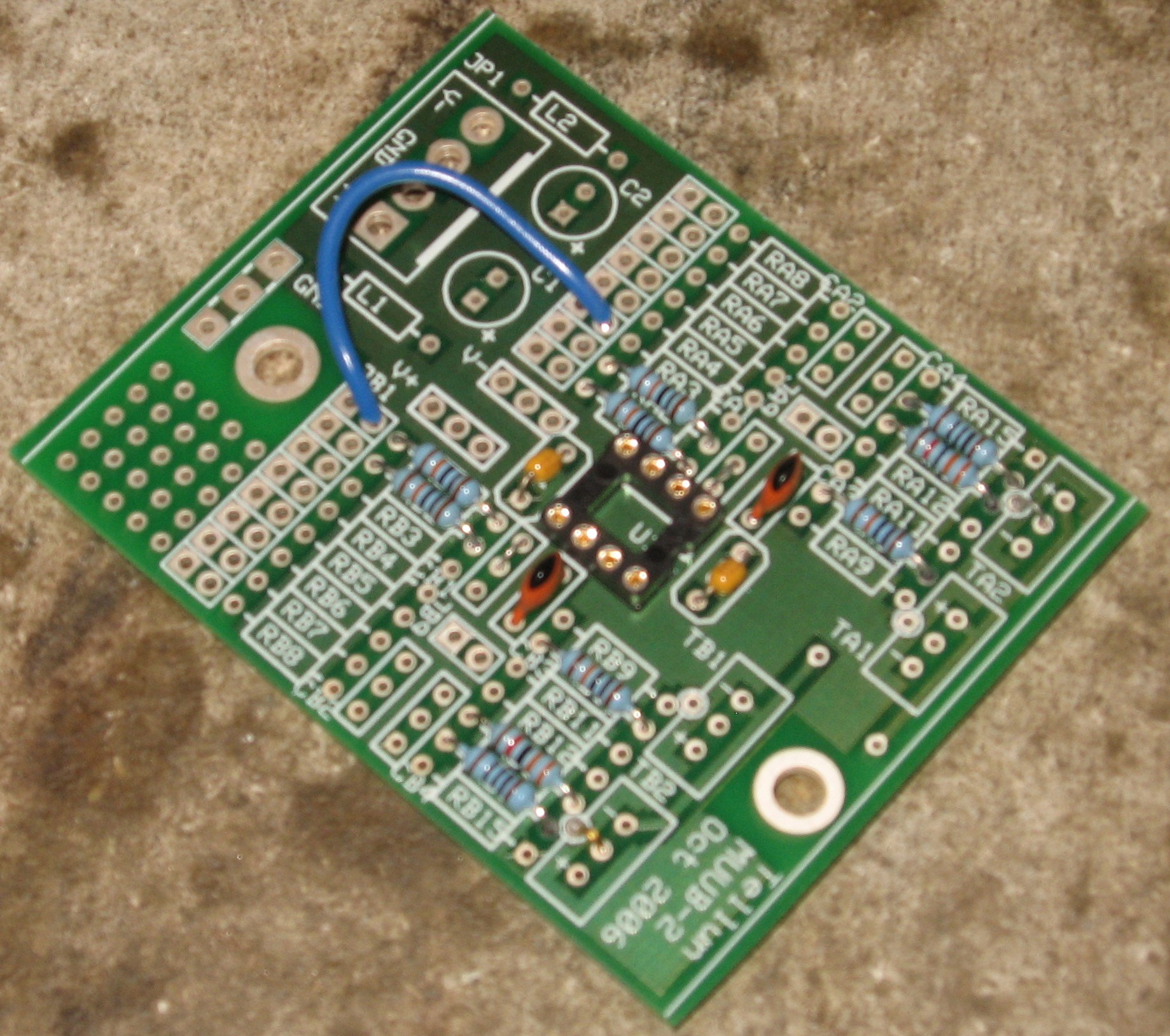
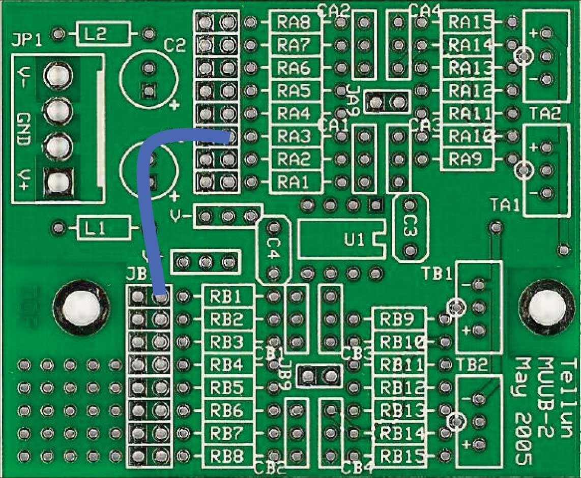
You're supposed to strip one end of the wire long - the end that goes in to the signal (round) pad at JA2 - so it can be folded down behind JA1. This way when you're connecting the wires later on, it will be there (so this wire jumper and RA1 will be joined). We didn't do this so we had to add a jumper later... much less elegant, but it worked.
PCB3 all done |
|
Construction - PCB4 PCB4 is built using an MUUB2 and is described in Scott's 861 User's guide section 5.7. For detailed drawings of the MUUB2, click here. Here's Scott's picture of Board 4 finished:
|
|
|
Phase 1 All the stuff in Phase 1 gets soldered using "Organic" Solder. At every break in the action, we wash the board off to get rid of the flux. |
|
|
Jumpers |
|
|
|
|
|
Resistors |
|
|
|
|
|
Capacitors |
|
|
Misc |
Misc stuff for PCB 4
|
|
Phase 2 The stuff in Phase 2 gets soldered using "No-Clean" Solder and the PCB doesn't get washed off from here on. |
|
|
Wire jumpers |
Similarly to PCBs 3, you're supposed to strip one end of the wire long - but here, it's the end that goes in to the signal (round) pad at JA3 - so it can be folded down behind JA2 and JA1. This way when you're connecting the wires later on, it will be there (so this wire jumper, RA2, and RA1 will be joined). We didn't do this so we had to add a jumper later... much less elegant, but it worked.
PCB4 all done |
|
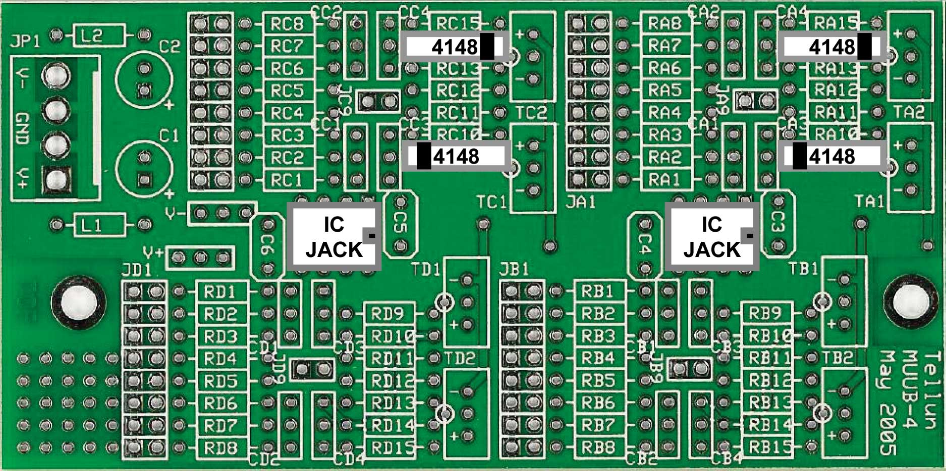
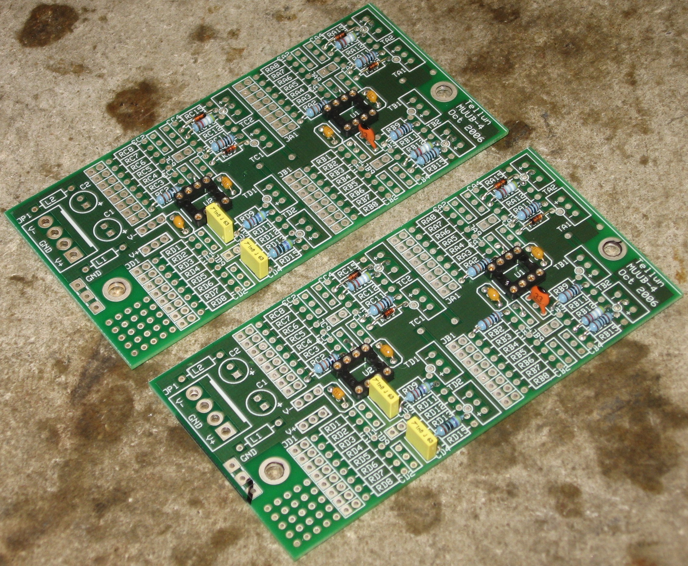
ICs |
|
|
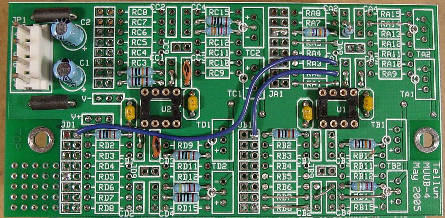
We put the TL072s into their sockets.
| |
|
Connection Wiring |
|
|
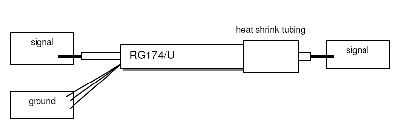
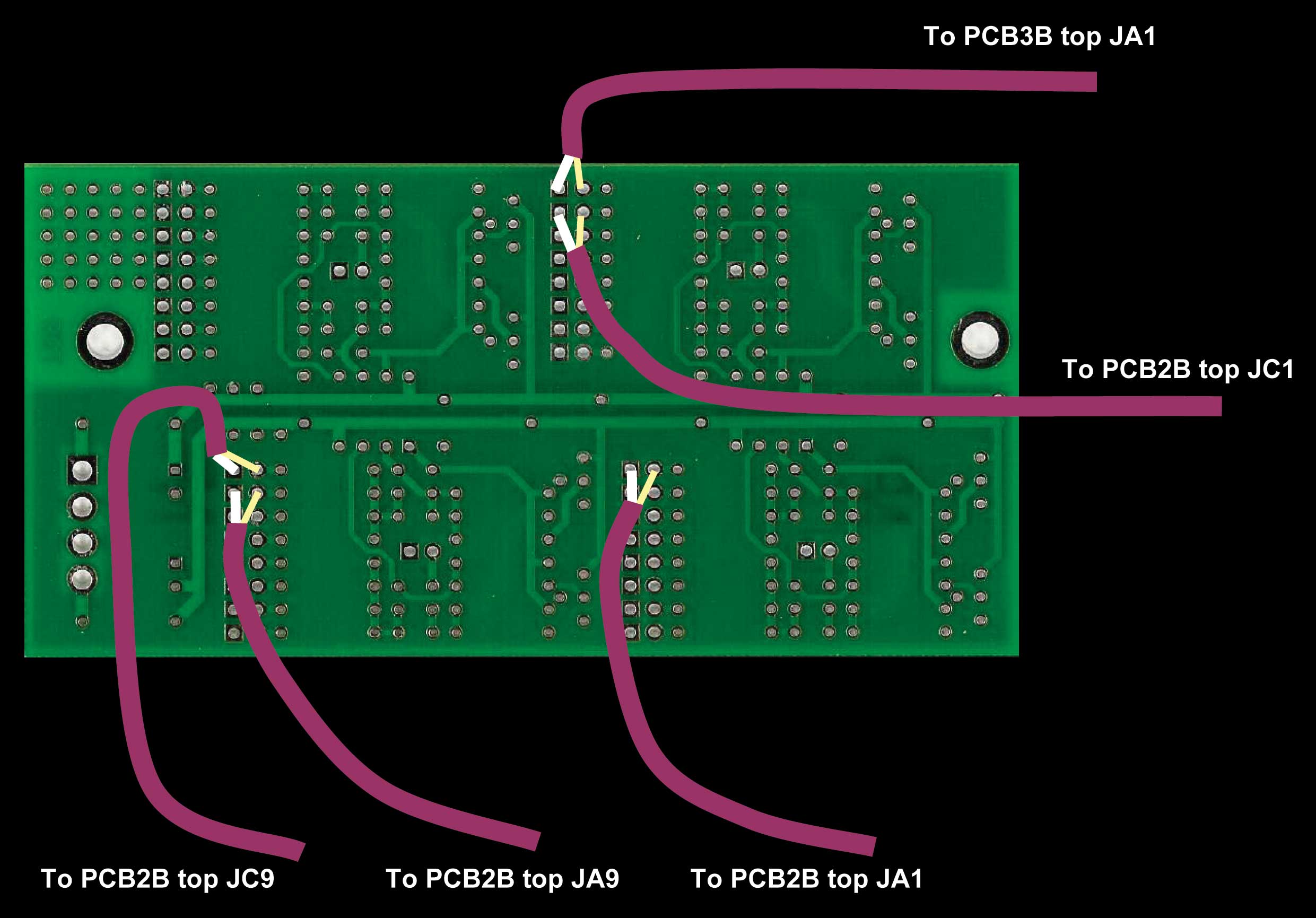
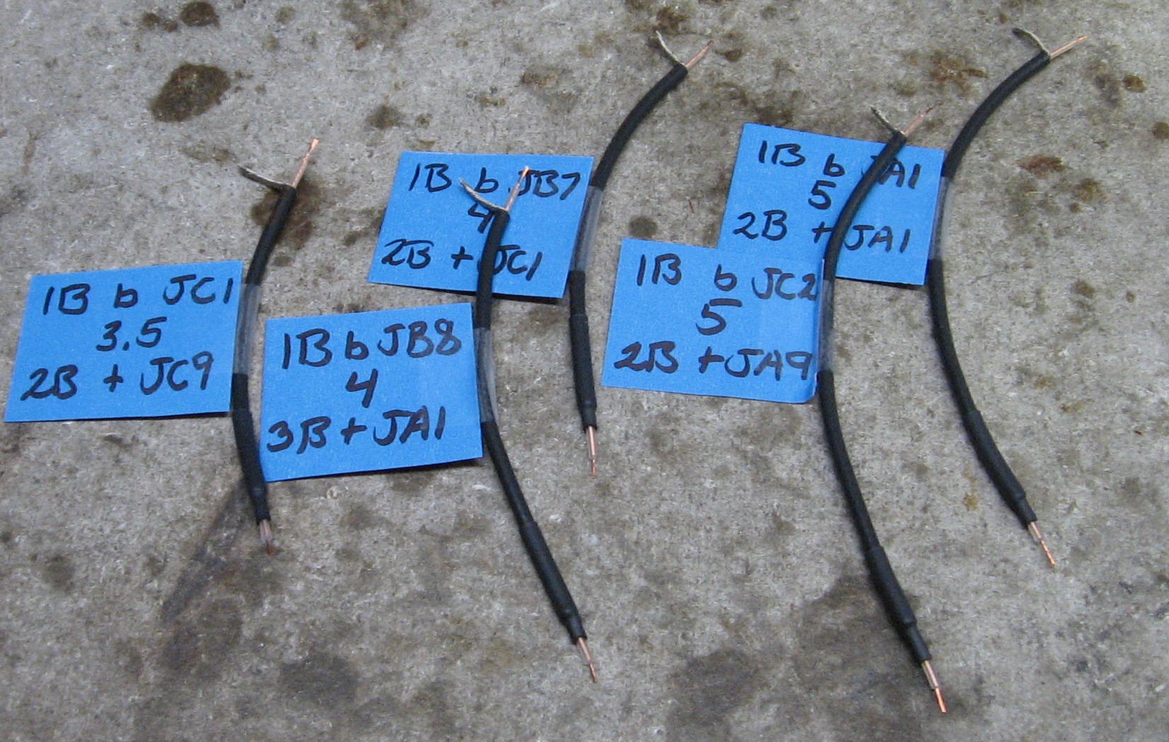
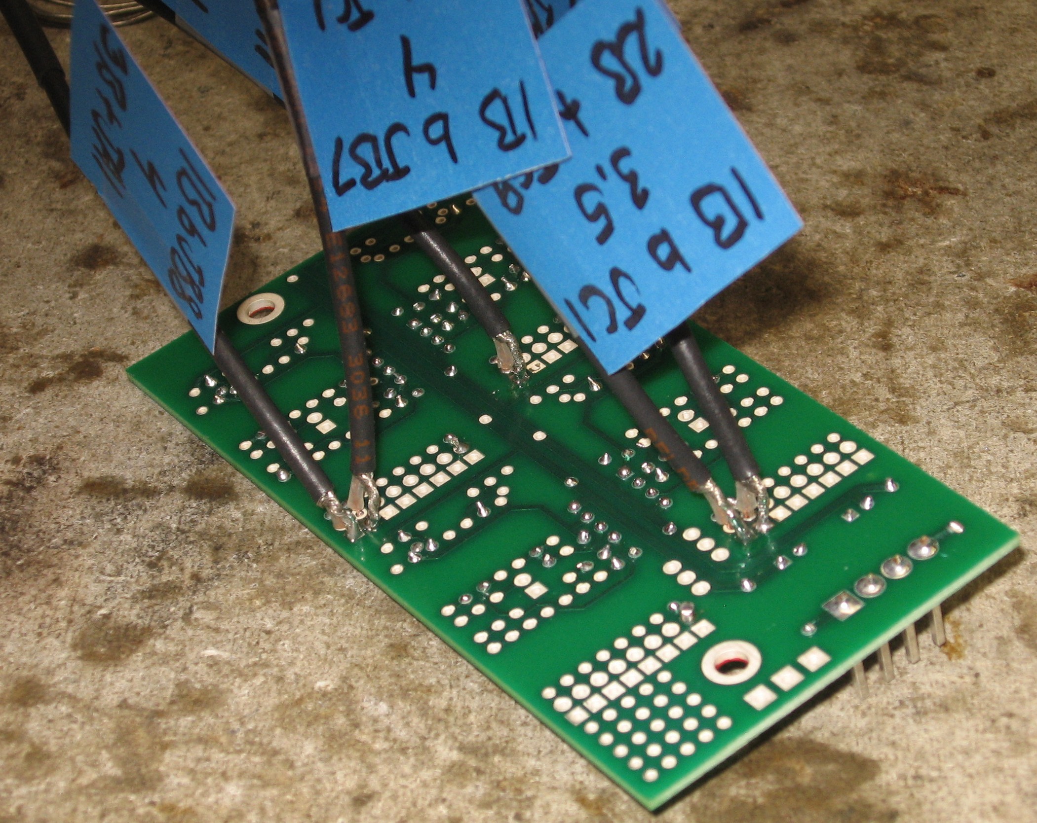
OK - the next step is to install the wiring that will make the connections between the PCBs and to the panel jacks. This is described in Scott's 861 User's guide section 5.9 "Board to Board Wiring" and section 5.10 "Board to Panel Wiring." All of these wires are coax. The wires that go PCB-to-PCB solder in such that the shield is only soldered at one end. These will be prepared with a bit of heat-shrink at one end. Here's Scott's illustration of how to prepare the PCB-to-PCB coax:
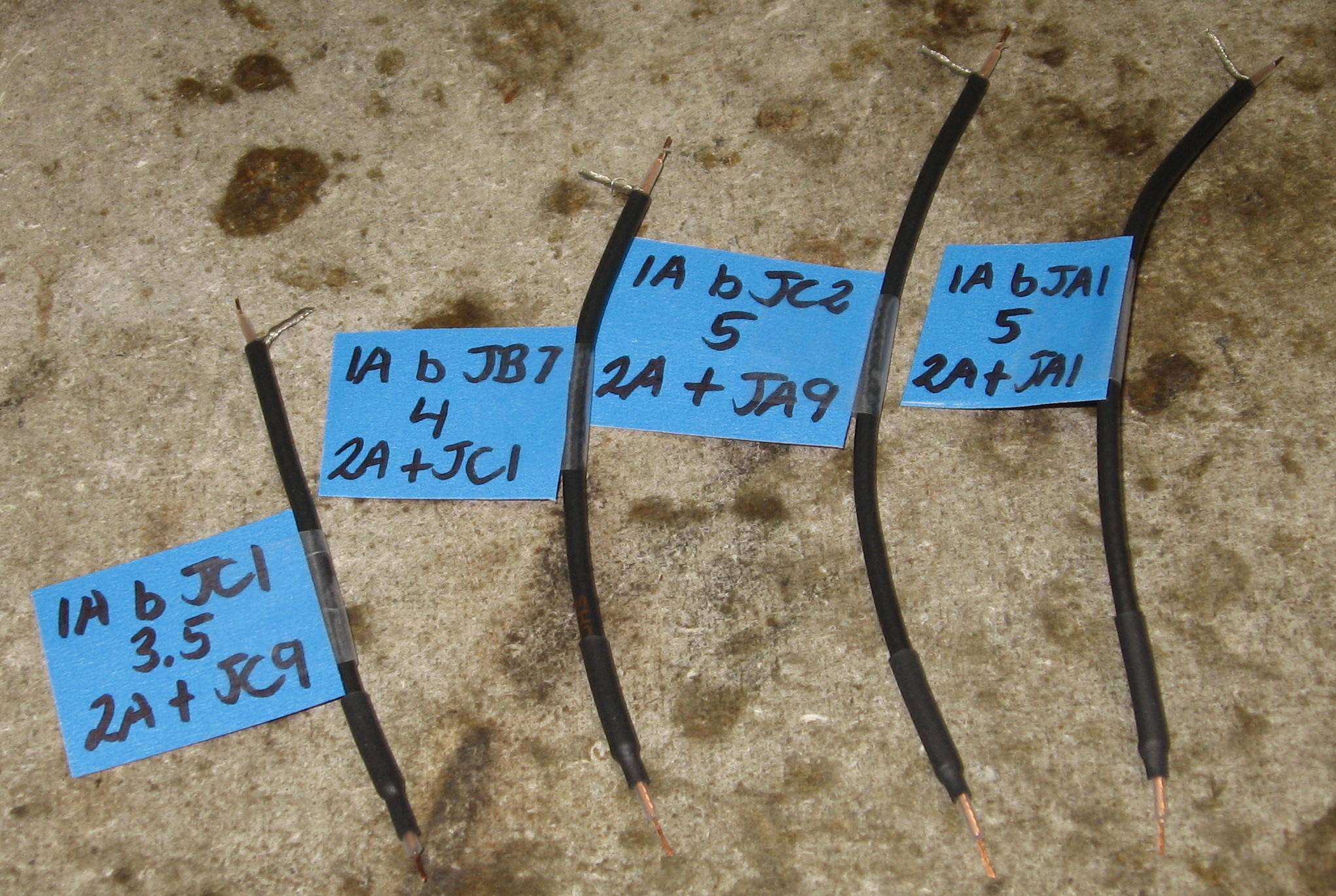
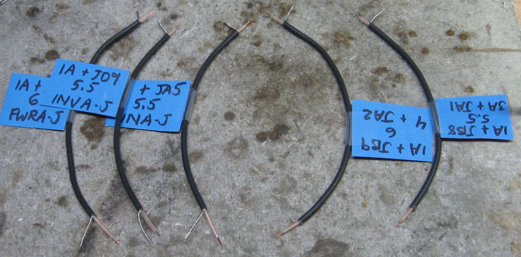
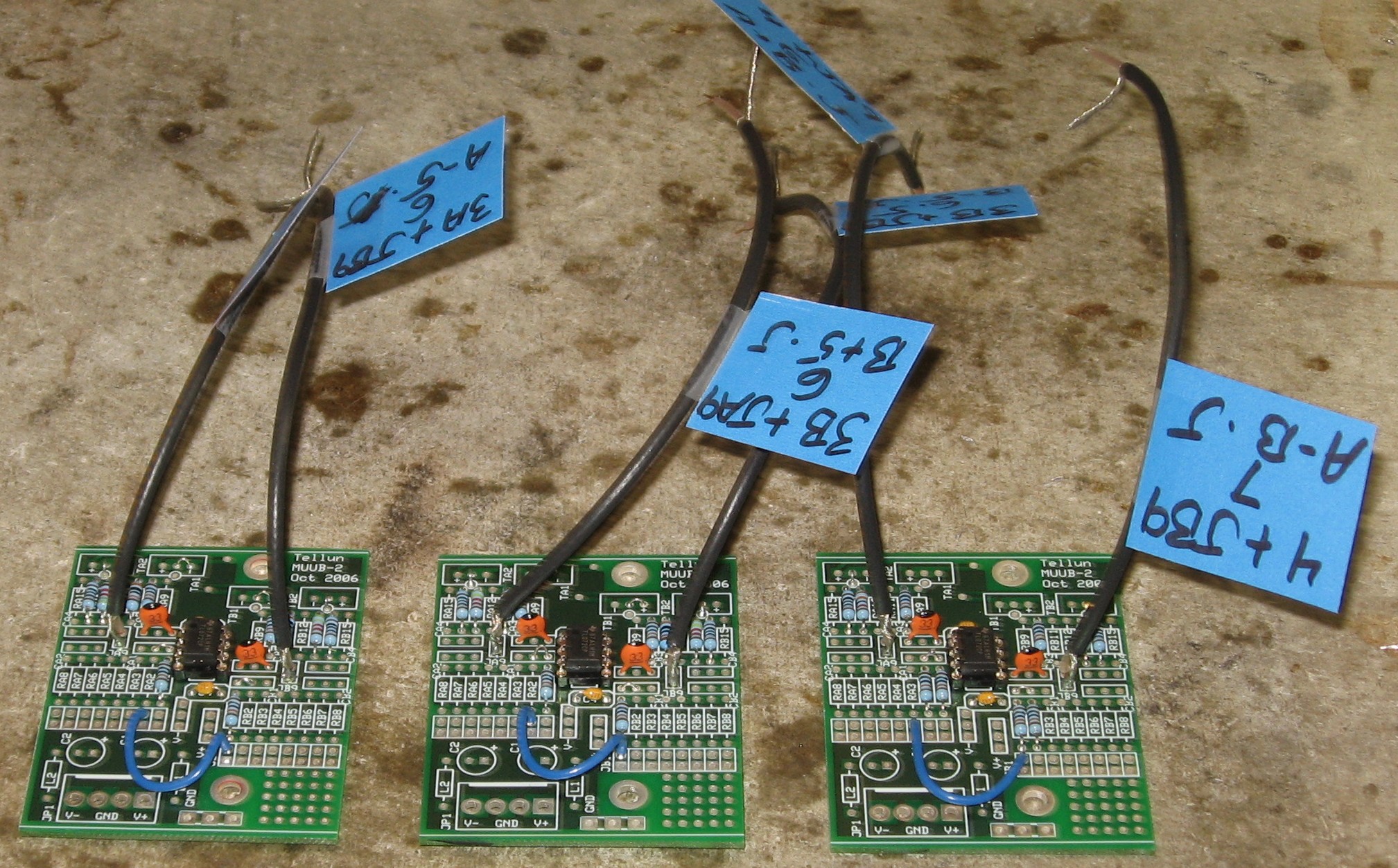
Of the jack-wires, double-check your anticipated position of the PCBs relative to the panel. You'll have to add length to the wires as required. We actually added an inch to the lengths described by Scott (and listed on this page). From this point on, all the PCBs are specifically different from each other. |
|
|
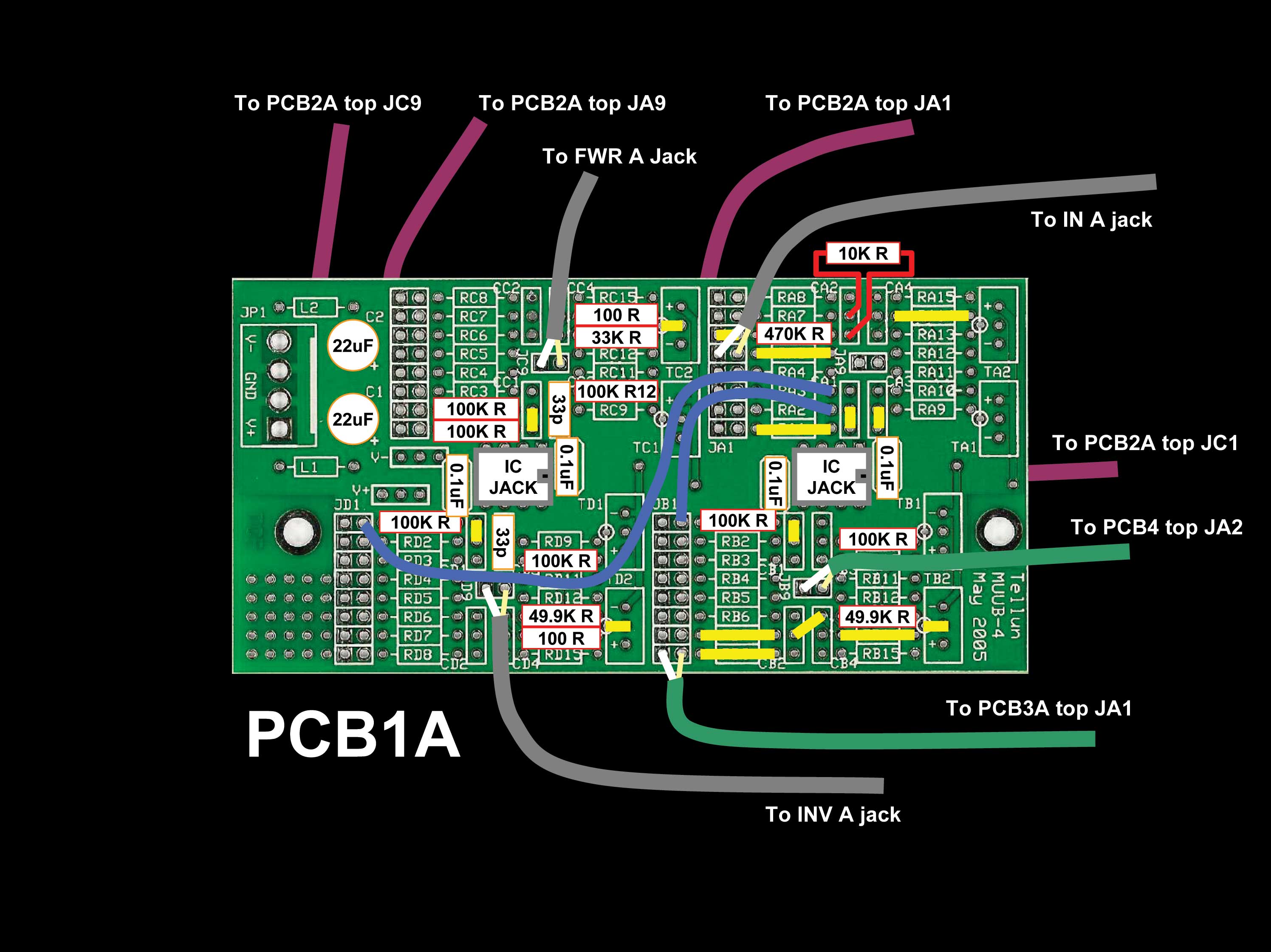
PCB1 A Bottom Wires |
|
|
OK, now - here are the wires that need to be soldered into the bottom of PBC1 A. All of these wires are Coax prepared so that the shield attaches at one end, and just the signal wire at the other end.
|
|
|
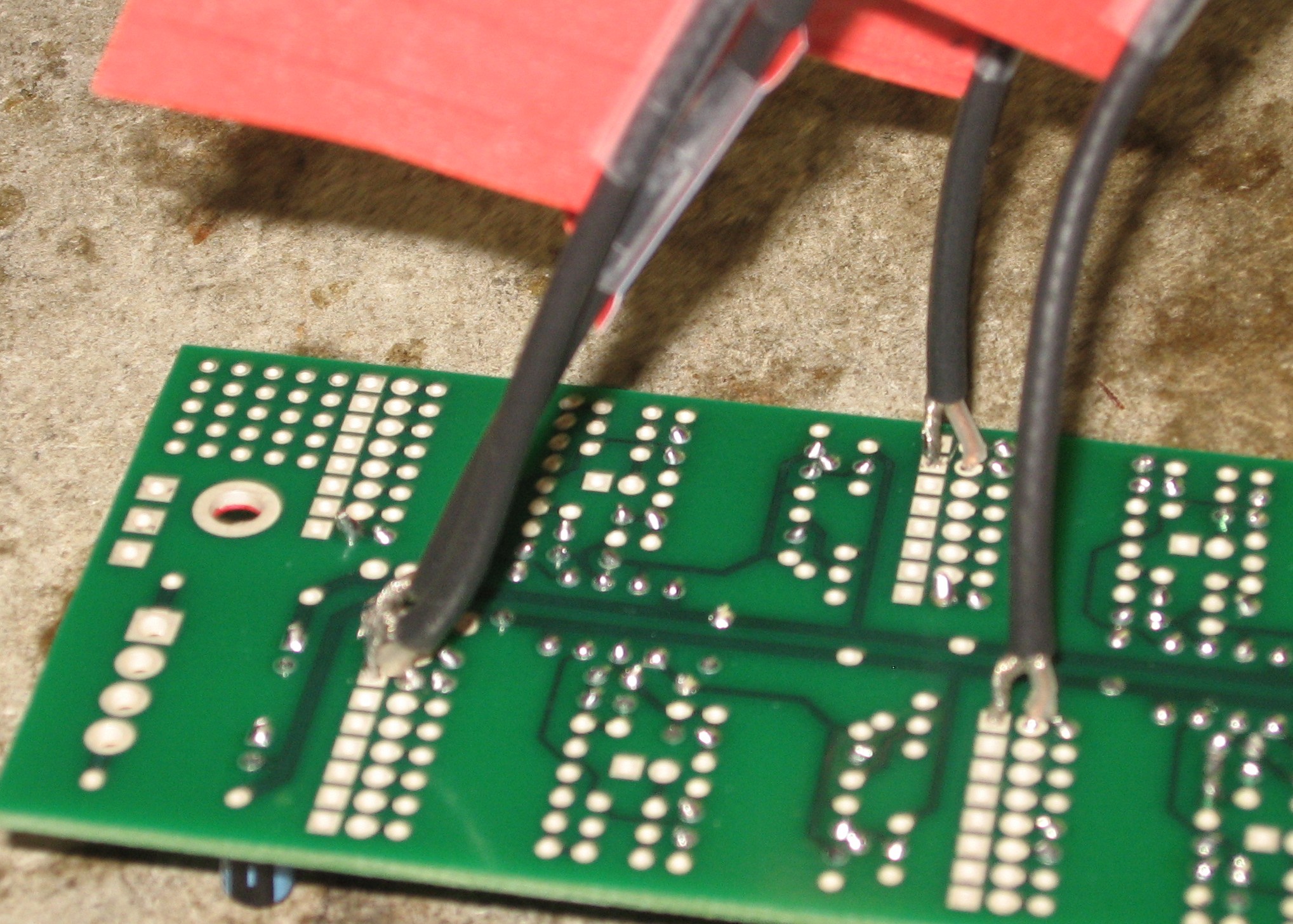
PCB1 A Top Wires |
|
|
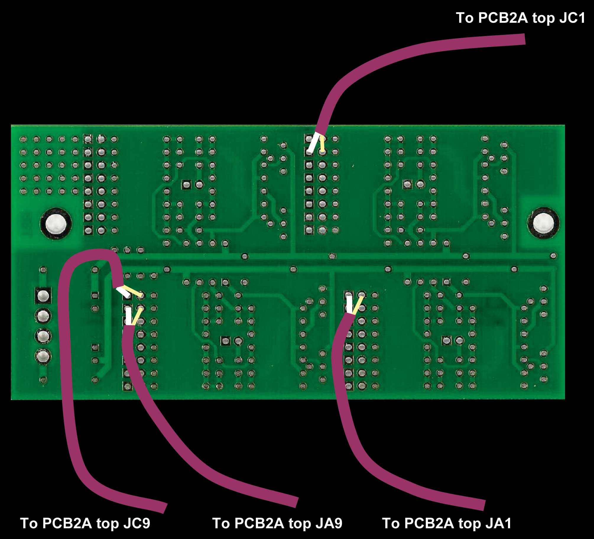
Here are the wires that need to be soldered into the top of PCB1 A. Again - all of them are coax - but here, three of them go to jacks.
|
|
|
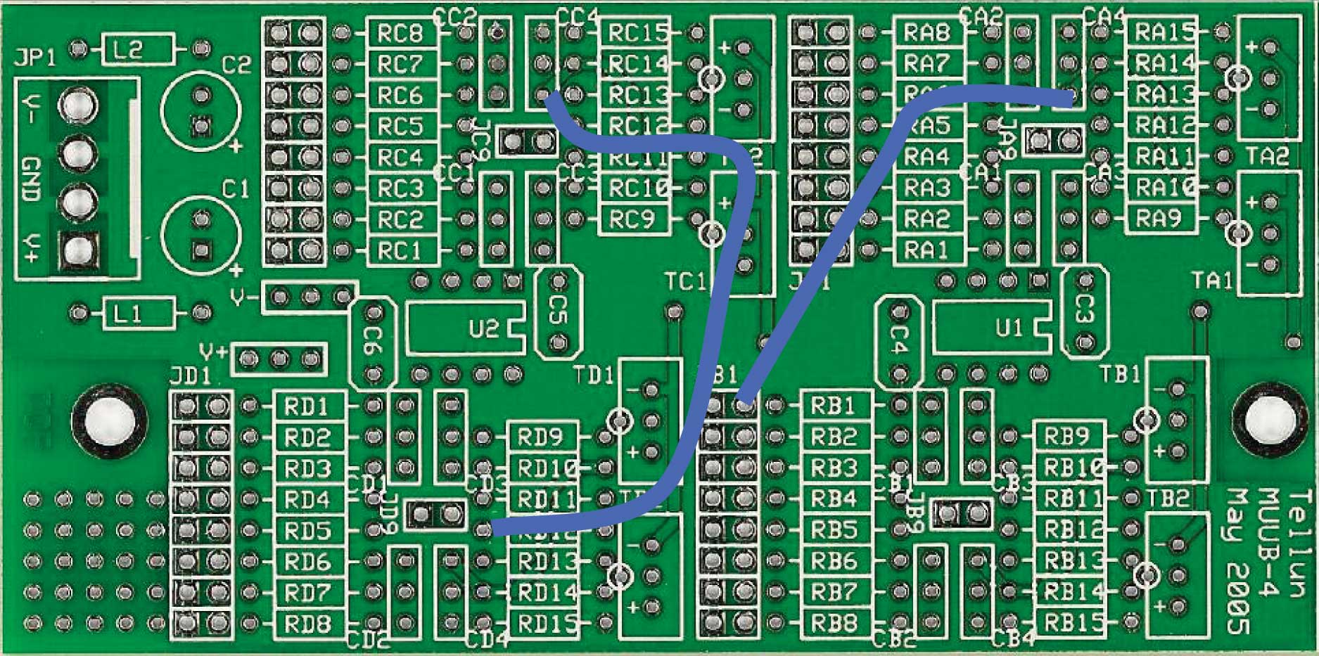
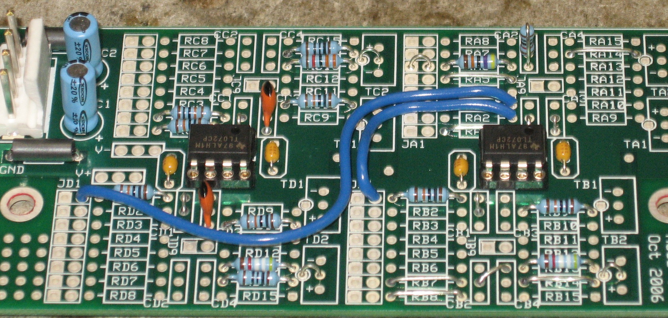
The Missing Jumper at JA6 |
|
|
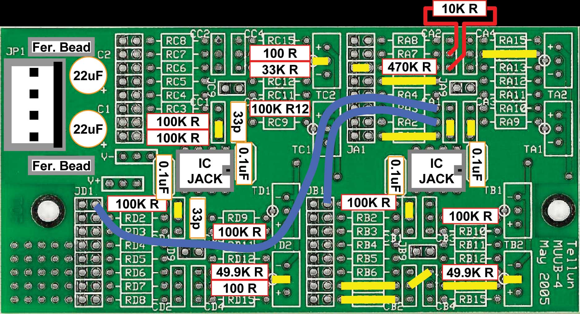
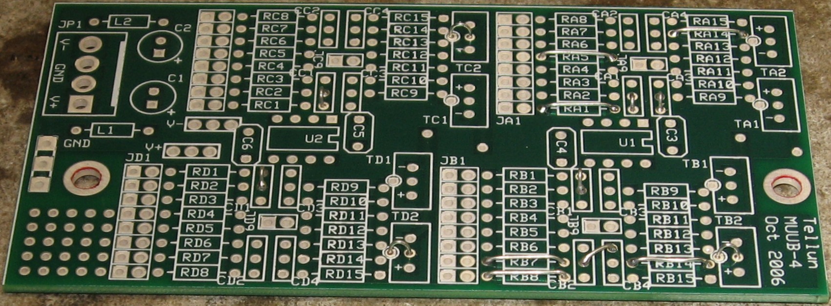
This is when we discovered our omission of the JA6 jumper on both PCB1 A & B. So we went back and soldered them into both PCBs using no-clean solder. You can see it in the photo of PCB1A, above - and we soldered it into PCB1B as well:
|
|
|
PCB1 B Bottom Wires |
|
|
OK - here are the wires that need to be soldered into the bottom of PBC1 B. All of these wires are Coax prepared so that the shield attaches at one end, and just the signal wire at the other end.
|
|
|
PCB1 B Top Wires |
|
|
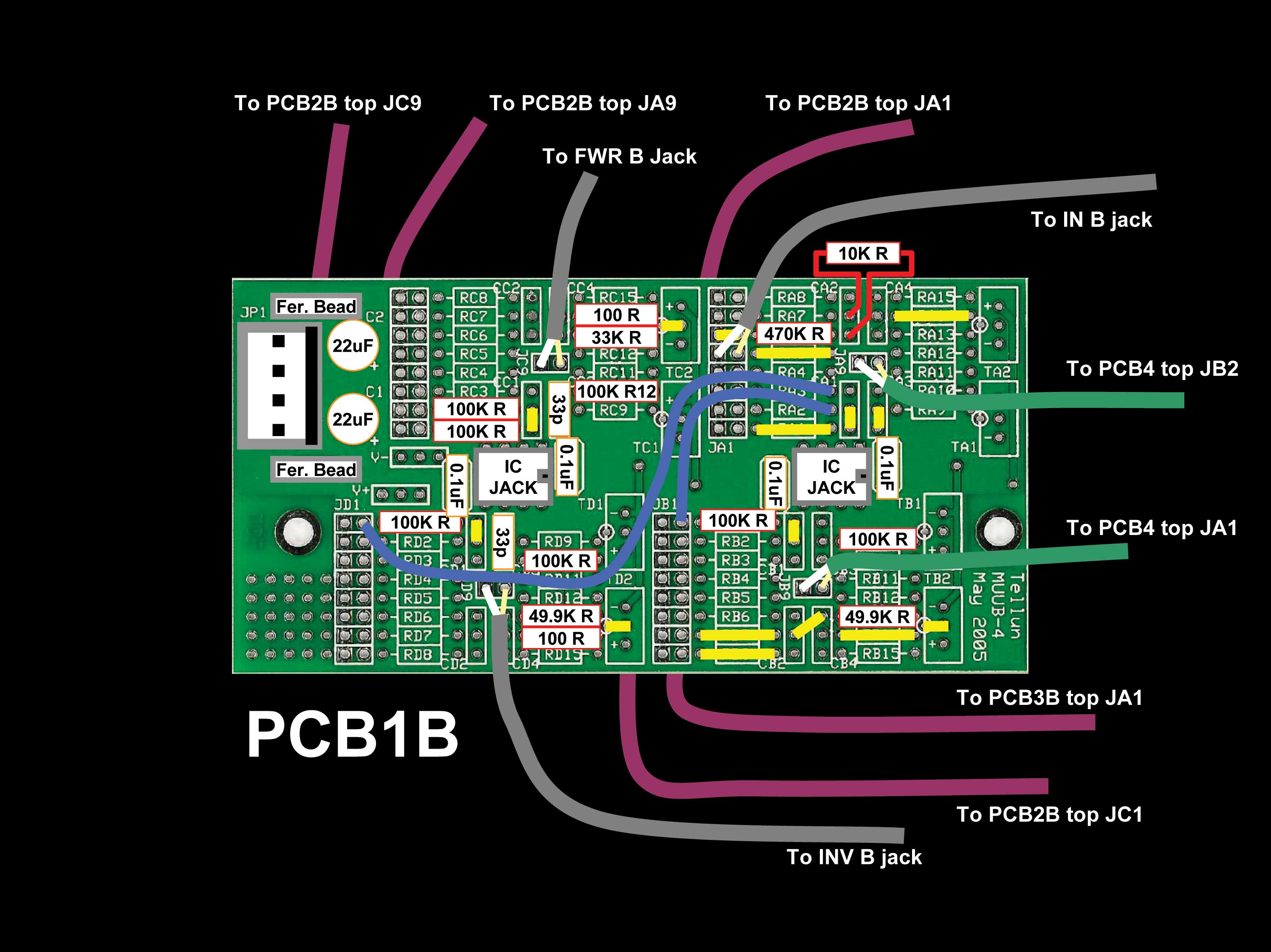
Here are the wires that need to be soldered into the top of PCB1 B. Again - all of them are coax - but here, three of them go to jacks.
|
|
|
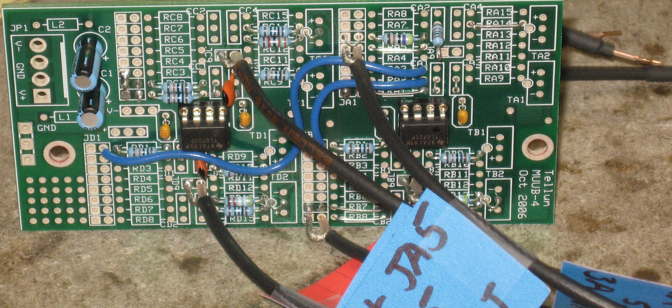
PCB2 A |
|
|
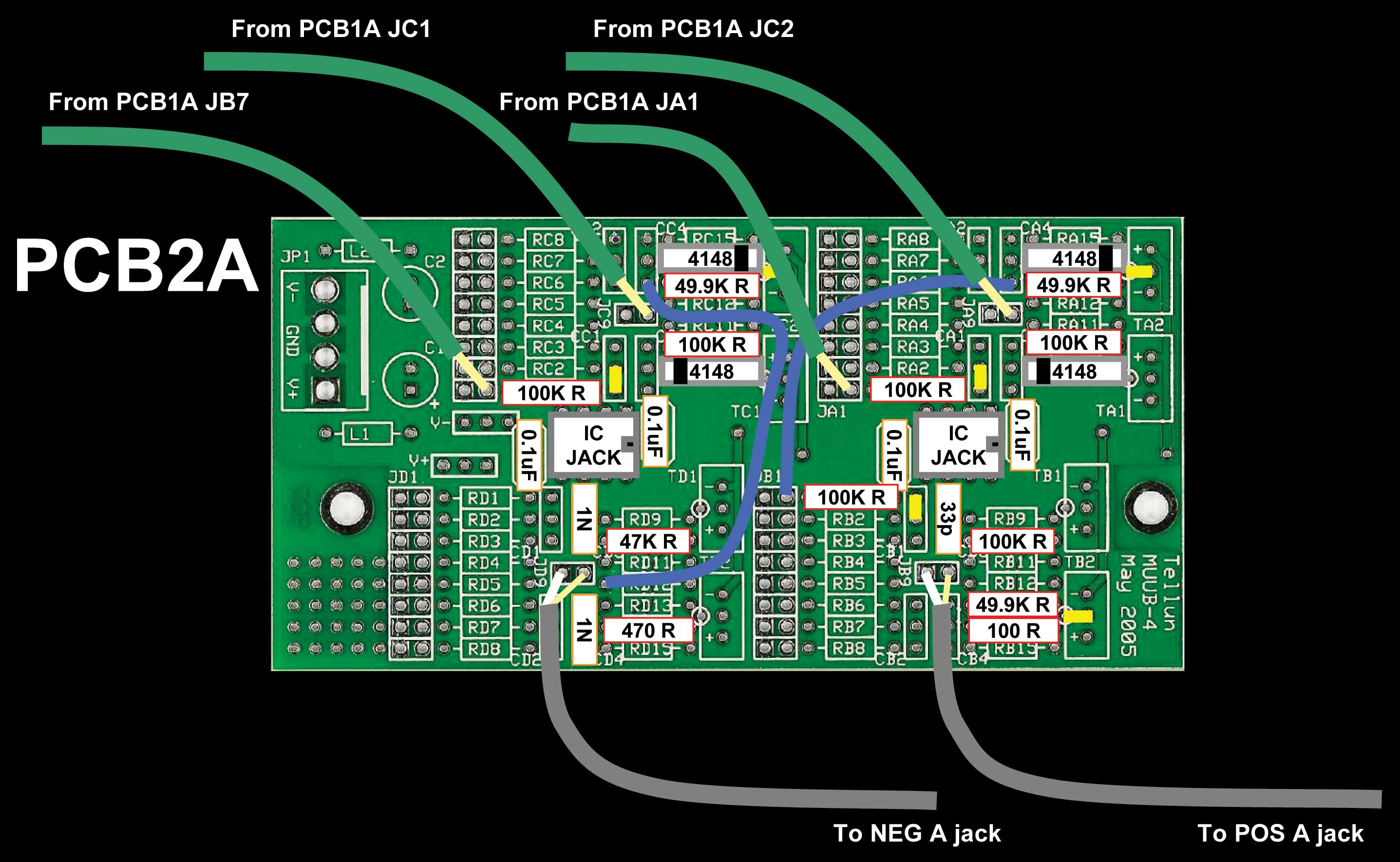
Here are the wires that need to be soldered into the top of PCB2 A. Four of the wires come from other PCBs but for now, we're just going to wire up the two jacks.
|
|
|
PCB 2 B |
|
|
Here are the wires that need to be soldered into the top of PCB2 B. Four of the wires come from other PCBs but for now, we're just going to wire up the two jacks.
|
|
|
PCB 3 A |
|
|
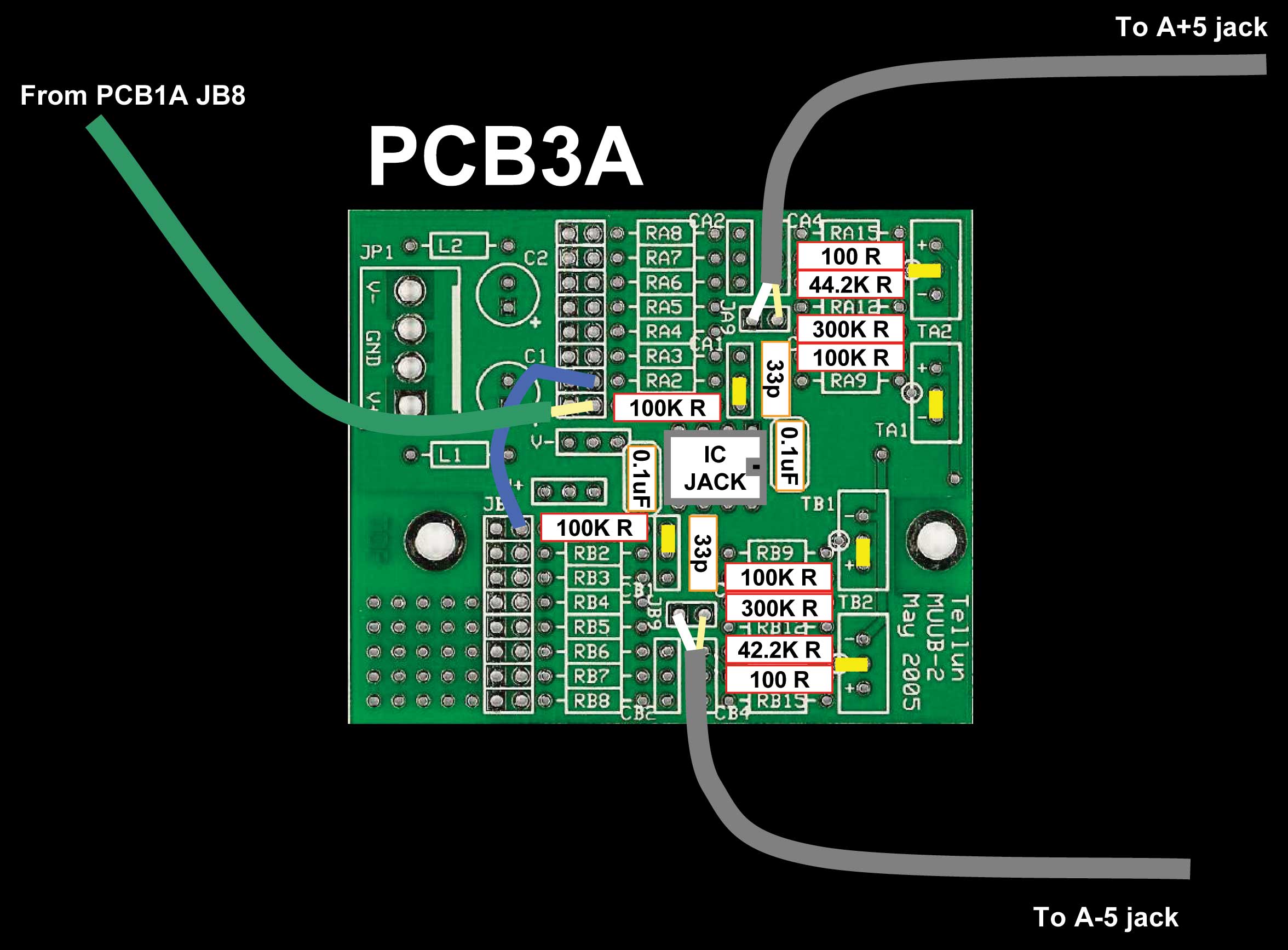
Here are the wires that need to be soldered into the top of PCB3 A. One of the wires come from another PCB but for now, we're just going to wire up the two jacks.
|
|
|
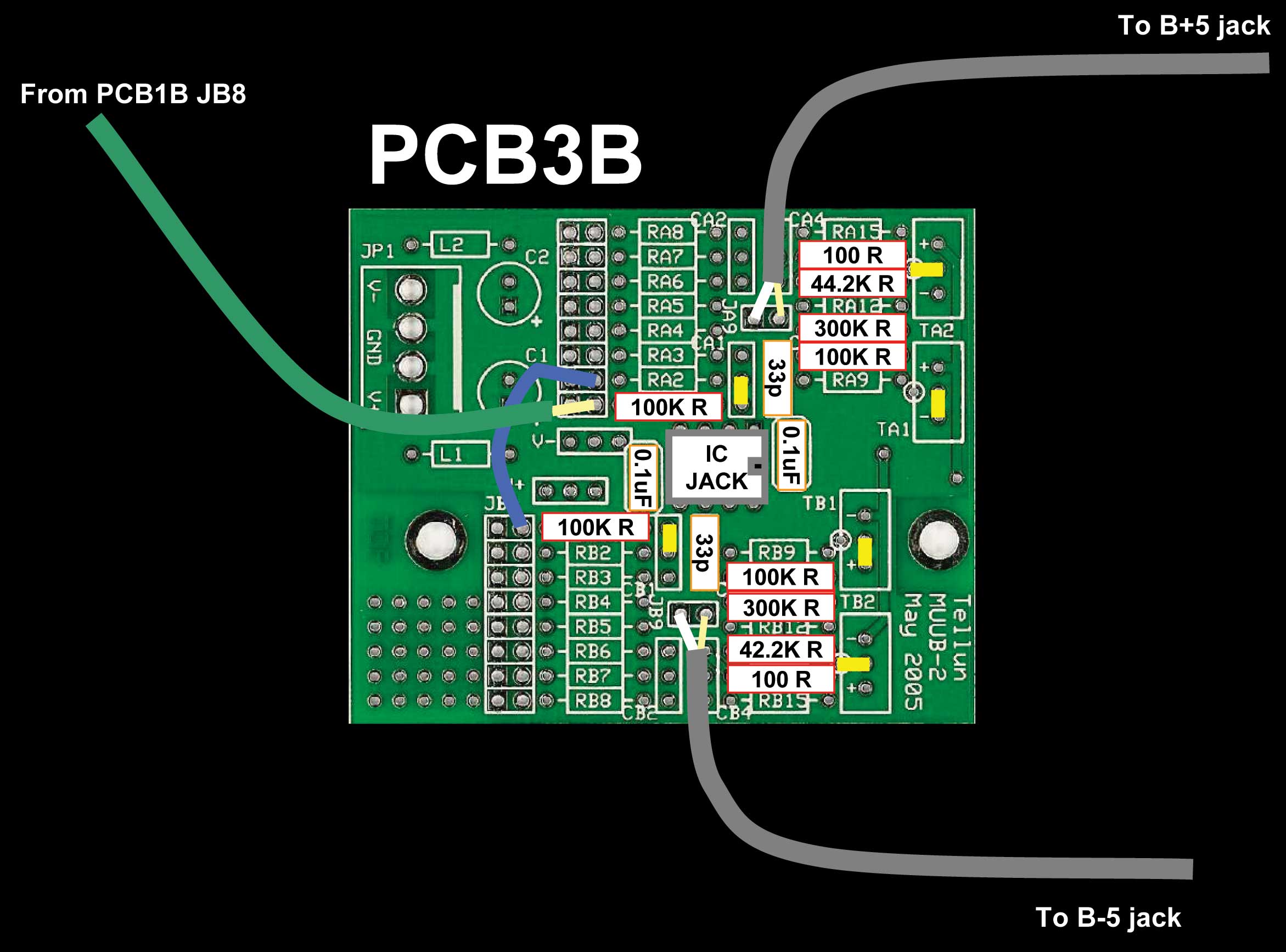
PCB3 B |
|
|
Here are the wires that need to be soldered into the top of PCB3 B. One of the wires come from another PCB but for now, we're just going to wire up the two jacks.
|
|
|
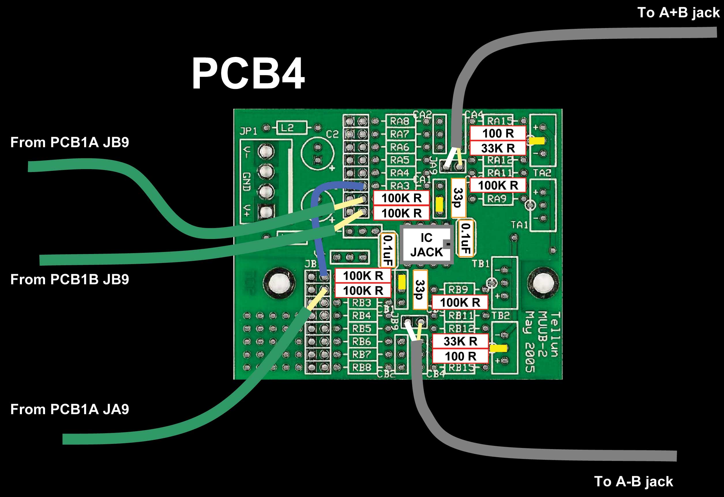
PCB 4 |
|
|
Here are the wires that need to be soldered into the top of PCB4. Three of the wires come from other PCBs but for now, we're just going to wire up the two jacks.
|
|
|
Same routine - measure, label, solder. |
|


|
The fine Print: Use this site at your own risk. We are self-proclaimed idiots and any use of this site and any materials presented herein should be taken with a grain of Kosher salt. If the info is useful - more's the better. Bill and Will © 2005-2011 all frilling rights reserved
|